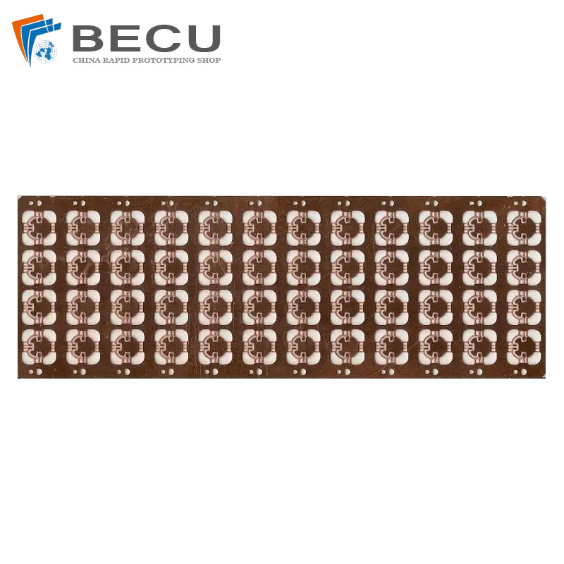
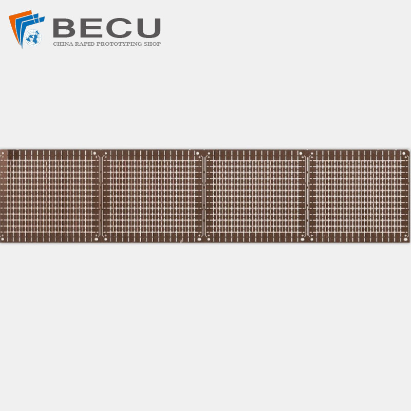
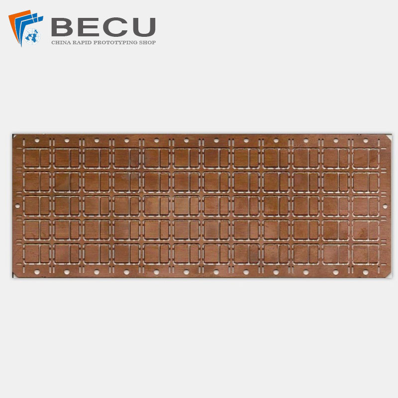
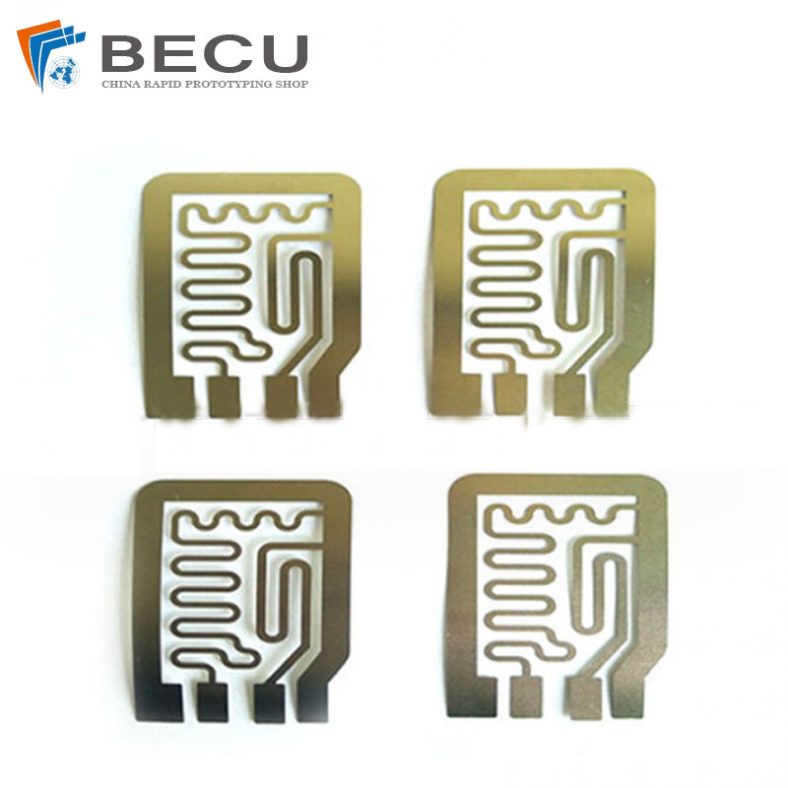
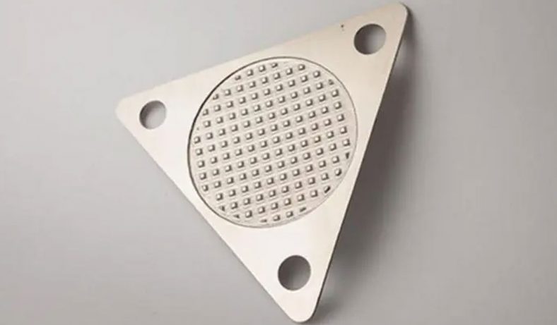
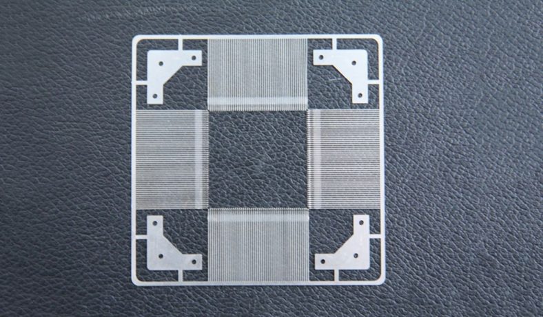
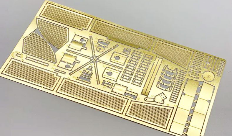
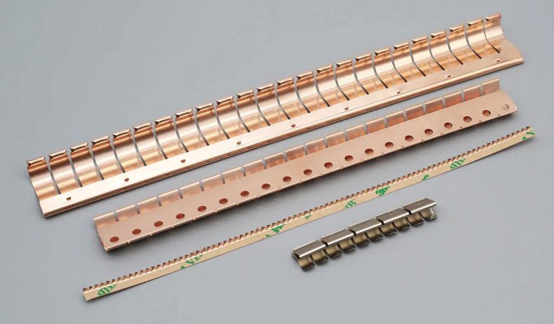
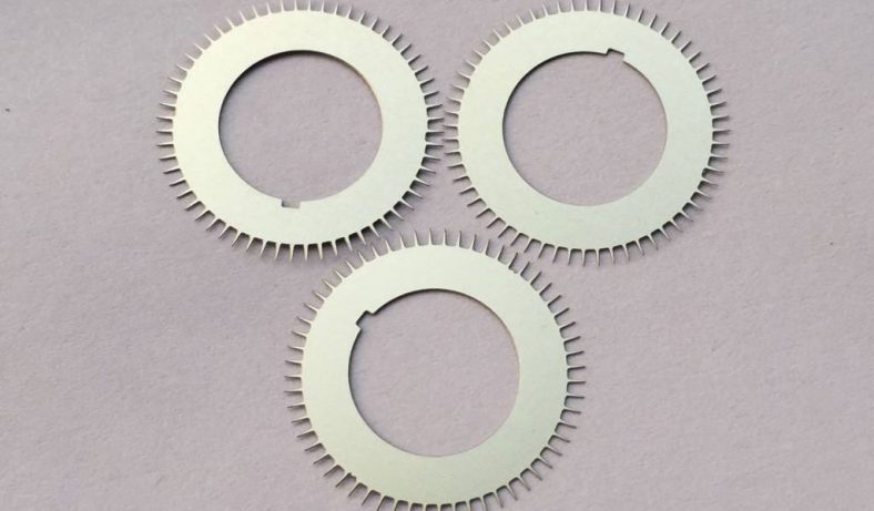
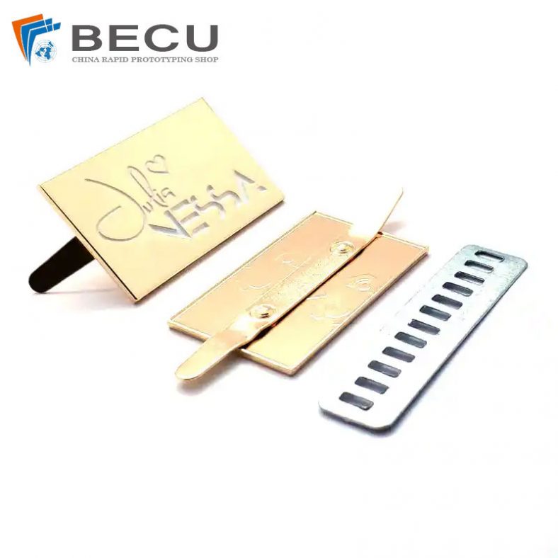
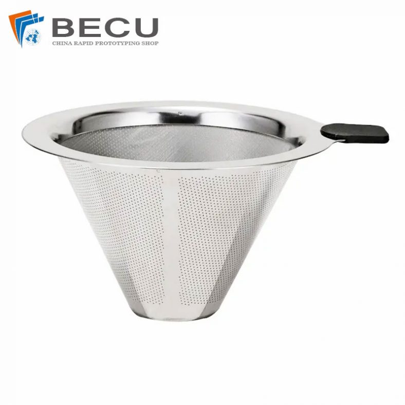
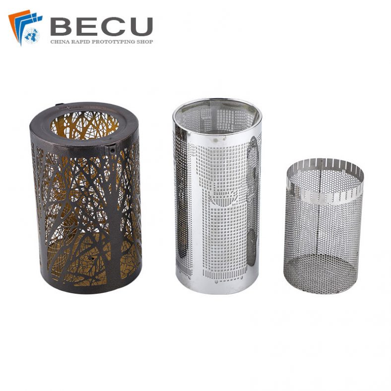
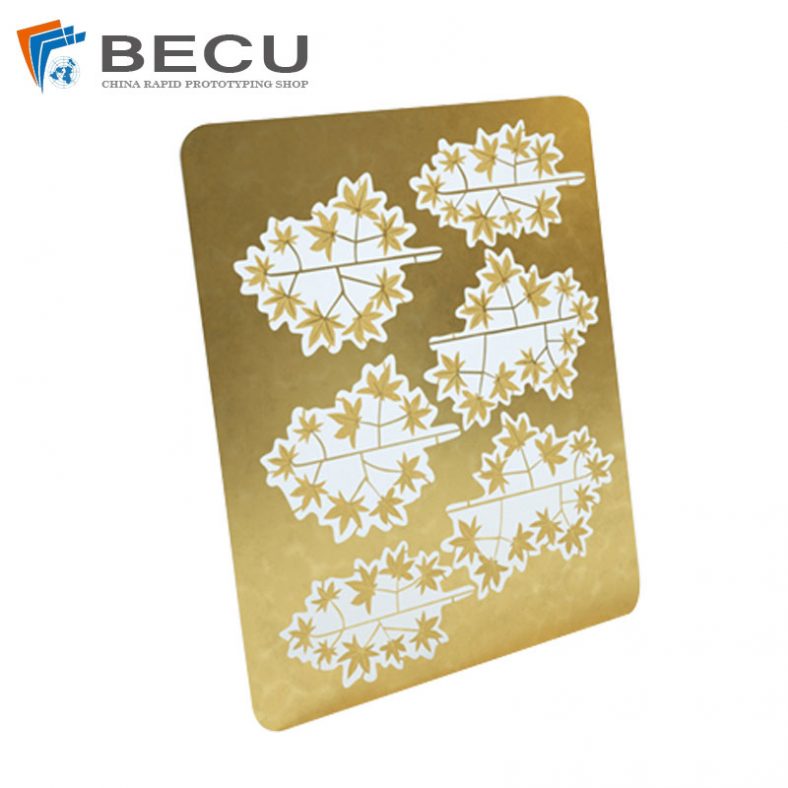
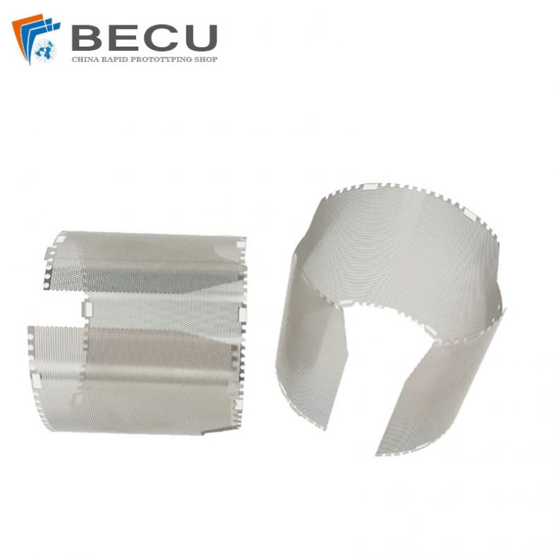
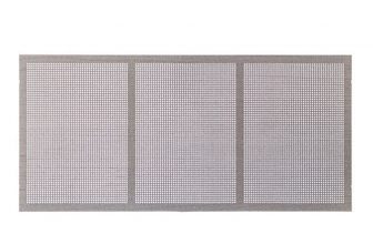
IC Lead Frame
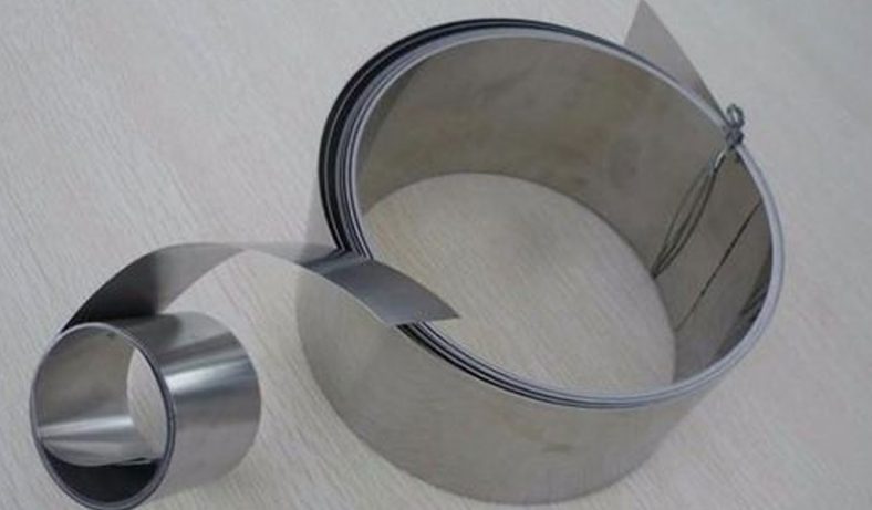
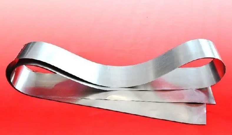
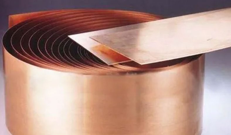
- Material: Copper alloy
- Thickness: 0.5/0.6/0.7 mm
- Project Offer:Within 3 hours
- Process: Precision Etching
- Custom Cycle:Involving Mold Opening, – monthly sample delivery
- Production Capacity:5000-10000PCS/day
- Application: Semiconductor Packaging
- Add Process:Stamping, Self-Owned Hardware Mold Room, Electroplating, Electrophoresis, PVD Vacuum Plating
- Type: Kovar Etching
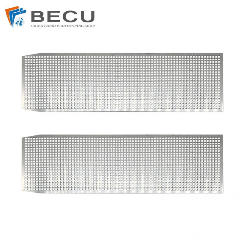
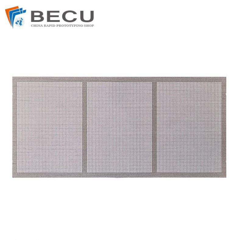
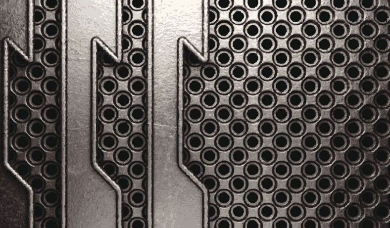
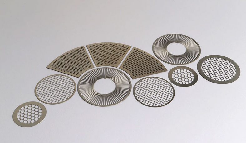
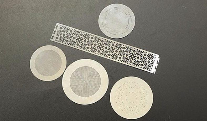
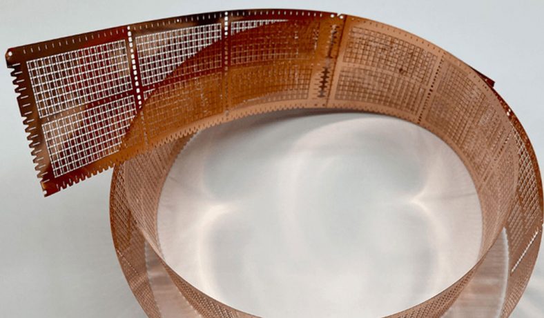
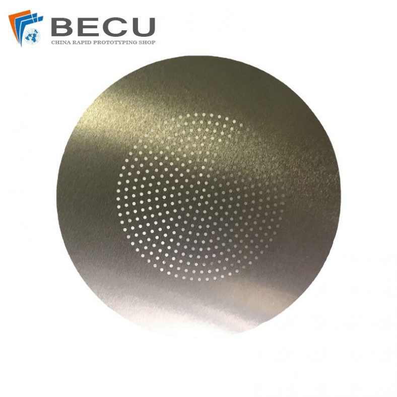
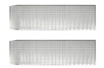
High-Quality IC Lead Frame and VFD Dedicated Grid Etching
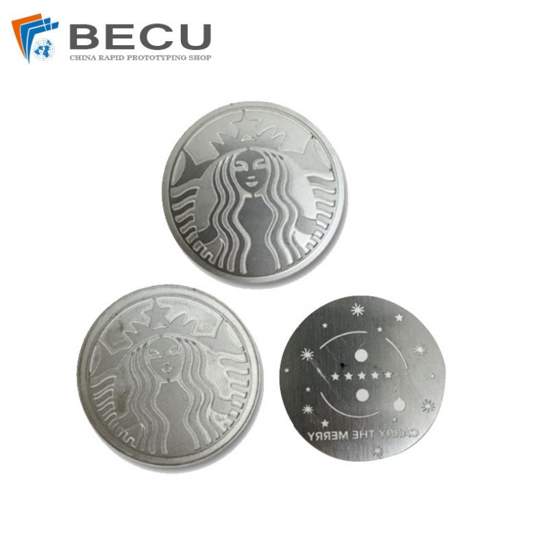
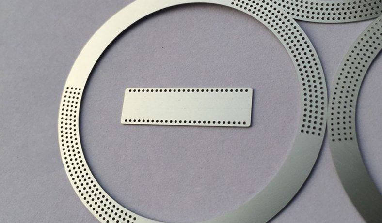
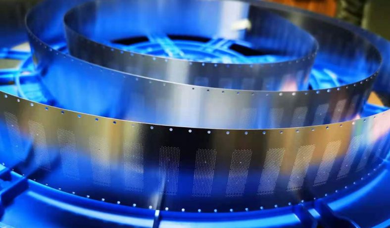
Lead frame etching is a widely used processing technology in the field of microelectronics. Its principle is to form a wire structure of a certain shape and size on the conductive layer through multiple processes such as masking, exposure, and development of the thin film. This processing technology is widely used in integrated circuits, MEMS and other fields. Its processing accuracy reaches the submicron level and has become an indispensable part of today’s microelectronics manufacturing.
In the lead frame etching process, the most critical link is the mask technology. The quality of the mask directly determines the accuracy and reliability of the wire structure. In order to ensure the quality of the mask, scientists have developed a variety of mask materials and preparation processes. Among them, photolithography technology is currently the most widely used mask technology, and its resolution can reach the submicron level. It is known as the “soul” of microelectronics manufacturing.
Lead frame etching, this technology plays an important role in the field of microelectronics. It has high processing accuracy and low manufacturing cost, and has been widely used and concerned. Have you heard of this technology? Come and leave a message and share your thoughts with us!
Why Choose Our IC Lead Frame and VFD Dedicated Grid Etching Service?
- Etching processing technology is adopted, with high precision, up to ±0.008mm (different thickness of different materials). 15 years of professional precision etching processing factory, the quality is trustworthy.
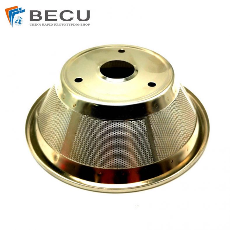
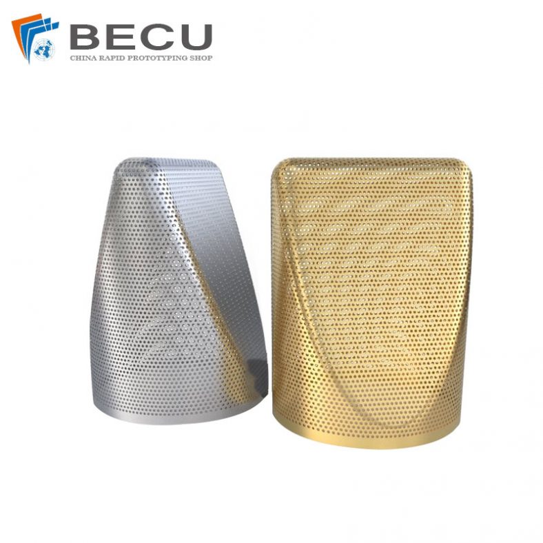
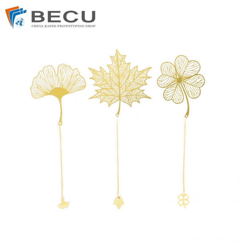
- The etching process of Be-cu has no restrictions on complex patterns and arbitrary geometric figures. No matter how complicated the hole shape or pattern is, it can be formed in one process without increasing the production cost.
- Be-cu chemical etching is a double-sided simultaneous processing technology. The surface of the product (front and back) is smooth, no bumps, no pits, no burrs, no warping, the mesh is flat and no deformation, no need to polish , Polishing, self-care process after flattening.
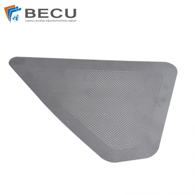
- The size of etching process is fine (aperture ≥ 0.1mm, thickness 0.03-2.0mm), and the positioning is accurate (minimum precision ± 0.008) uniform.
- The production cycle is short, the response is fast, and the design is easy to modify. The Be-cu professional etching technology engineering team has a total of 17 people and has senior technicians who have been in the industry for 15+ years.
- Be-cu samples are produced quickly, and samples can be produced within 1-2 working days (determined according to product requirements).
- Be-cu etching has 16 automatic etching production lines, with high etching processing output, which can meet your production orders for batch processing and etching customized microporous mesh.
- Be-cu provides auxiliary services such as stamping, welding, oil spraying, painting, electrophoresis, electroplating, electrolysis, passivation, polishing, stretching, wire drawing, silk screen LOGO, injection molding, etc., to meet the needs of different products and realize convenient and fast — One-stop processing service.
- Be-cu has passed the factory inspections of many well-known companies such as Gree, Joyoung, Xinbao, Xiaomi, Lake and American and German customers. The quality and delivery time are stable, and the customer satisfaction and employee satisfaction are high.
Contact Be Cu Now for your Custom Metal Etching, We are your best online Etching services choice!
Specifications of IC Lead Frame and VFD Dedicated Grid Etching
| Material Type | Aluminium/Brass/Copper/Nitinol/Stainless steel/Titanium |
| Size | Customized |
| Min. Hole Dia. | Dia.≥1.2xT |
| Min. Pitch | D≥1.0xT |
| Tolerance | 0.003mm |
| Material Thickness | T≥0.03mm |
| Process | Etching/Plating/Stamping/Bending/Laser cuting |
| Surface Finish | PVD/Coating/Painting |
| Inspection | IPQC/AQL |
| Packing | Plastic Tray or Customized |

