
Homepage » Metal Etching »
What Is Selective Etching
Selective etching is a material processing technique used in various industries, including microelectronics, metallurgy, and materials science. It involves the controlled removal of specific areas or regions of a material’s surface while leaving the rest of the material unaffected.
This process relies on the principle that different materials or crystallographic orientations exhibit varying rates of dissolution or removal when exposed to specific etchants.
Selective etching finds widespread applications in a variety of industries and scientific fields. It is commonly used in semiconductor manufacturing to define features on microchips, in metallurgy to reveal microstructural details in metal samples, in micro-electro-mechanical systems (MEMS) and nano-electro-mechanical systems (NEMS) for creating tiny mechanical and electrical components, and in photovoltaics to improve the efficiency of solar cells, among many other uses. This technique provides a high level of precision and control in shaping, refining, and modifying materials for specific applications.
Custom Selective Etching – Selective & Half Etching
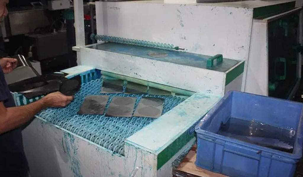
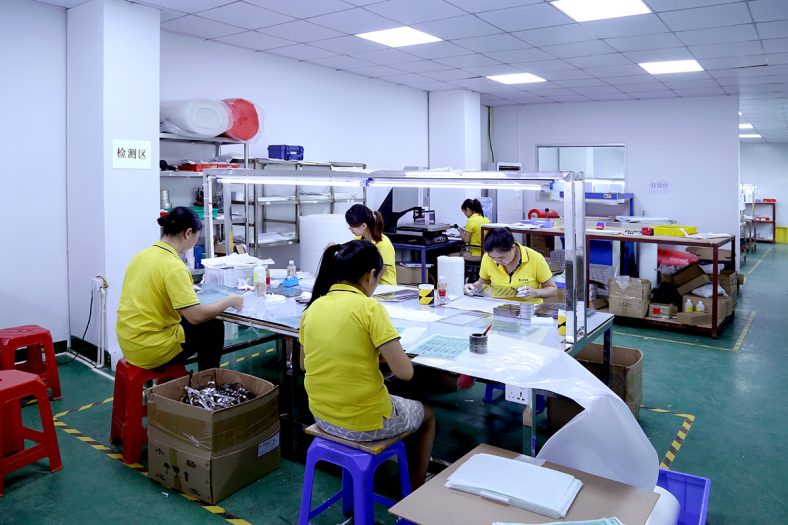
BE-CU ETCH is an expert providers of precision etching services in China. We are not only experts in providing selective etching, but also on half etching. The best thing about BE-CU is that we make use of the most advanced machinery in our state-of-the-art metal etching shop.
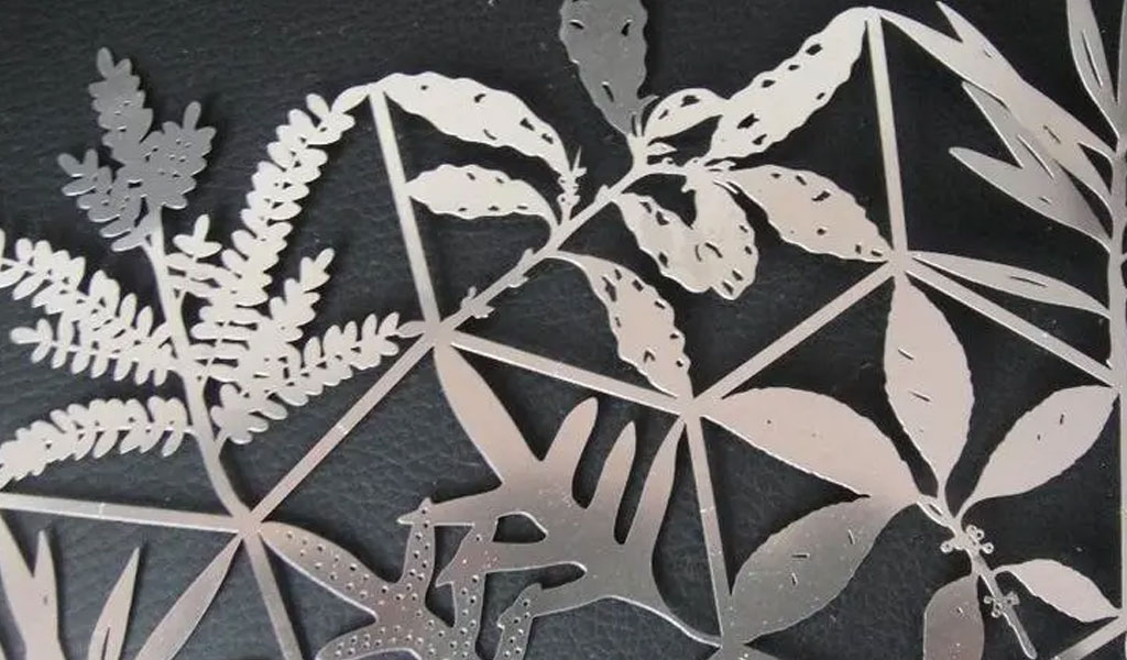
Manufacturer of thin selective metal etching parts produced to customer specifications utilizing photochemical milling. Secondary services include plating & forming. Burr-free & stress free parts.
Applications include washers, battery contacts, screens, RF shields & covers, electronic components, flex circuits, & decorative. Materials include copper, beryllium copper, stainless steel, brass, kovar, nickel & nickel silver, phosphorous bronze, cold rolled steel, & blue temp steel. Serves technological, medical, manufacturing, communication, metal stamping, computer, aerospace, & printing markets. From prototype to production. ISO 9001:2015 Certified.
We are fast increasing our presence across the global. We have clients in virtually every country.Be-Cu Tech can also serve you with our best-in-class products and services in other states of the US. Get a quote for your requirements here .We accept a variety of file formats. So, you can send us your requirements in various file formats, such as AutoCAD, DWG, IGES, STEP, PDF, SolidWorks, and DXF.
The Selective Etching Methods
Selective etching is a process used in materials science and semiconductor manufacturing to remove specific areas of a material while leaving other areas untouched. The type of selective etching used depends on the specific application and the material being etched. Here are some common types of selective etching techniques:
Wet Etching
Dry Etching
Anisotropic Etching
Isotropic Etching
Chemical-Mechanical Polishing (CMP)
Photochemical Etching
The choice of selective etching technique depends on factors such as the type of material, the desired etch rate, the required selectivity, and the specific application. Engineers and researchers select the appropriate method based on their specific needs and the properties of the materials involved.
Uses for Selective Etching
Selective etching is a versatile material processing technique that has a wide range of applications in various industries and scientific fields. Some of the key uses for selective etching include:
- Semiconductor Manufacturing: Selective etching is a fundamental process in the production of microchips and integrated circuits. It is used to define features, remove or shape materials such as silicon, silicon dioxide, and metals, and create intricate patterns and circuits on semiconductor wafers.
- Metallurgy: In metallurgy, selective etching is employed to reveal microstructural details in metal samples. This technique allows scientists and engineers to study the grain structure, defects, and phases in materials, which is essential for quality control, research, and understanding the properties of metals.
- Micro-Electro-Mechanical Systems (MEMS) and Nano-Electro-Mechanical Systems (NEMS): Selective etching plays a crucial role in the fabrication of tiny mechanical and electrical components in MEMS and NEMS devices. It is used to create small features and cavities in microdevices, such as sensors, actuators, and switches.
- Photovoltaics: Selective etching is used in the production of solar cells to texture the surface of silicon substrates. This texturing enhances light absorption, improving the efficiency of solar cells by reducing light reflection.
- Biotechnology: In the field of biotechnology, selective etching is employed to create microfluidic channels on substrates for lab-on-a-chip devices and other bioanalytical systems. These microfluidic channels enable precise control and manipulation of small volumes of liquids for various analytical and diagnostic applications.
- Surface Engineering: Selective etching is used to modify the surface properties of materials. It can make materials hydrophobic, hydrophilic, or customize their adhesive properties. This is particularly important in industries such as automotive, aerospace, and consumer products, where surface properties significantly impact performance and functionality.
- Integrated Optics: In the field of integrated optics, selective etching is used to create waveguides and optical devices. By etching specific regions of an optical substrate, light can be guided and manipulated within the material, enabling the development of compact and efficient optical components for telecommunications and data transmission.
- Chemical Sensing: Selective etching can be used to create microsensors with tailored surface properties. These sensors can selectively interact with specific molecules, making them useful for chemical sensing and detection applications.
- Electrochemical Systems: In electrochemical systems, selective etching can be employed to create structured electrodes and catalysts. This enhances the performance and efficiency of electrochemical reactions in applications such as fuel cells and batteries.
- Nanofabrication: Selective etching is used in the creation of nanoscale structures and devices, enabling precise control over the size and shape of nanomaterials for a wide range of applications, including nanoelectronics and nanophotonics.
These are just a few examples of the diverse applications of selective etching in various industries. Its ability to selectively modify the surface and structure of materials makes it a valuable technique for shaping and enhancing materials for specific functions and applications.
How is Selective Etching Accomplished?
Selective etching is accomplished through a series of well-defined steps that involve the controlled removal of specific areas of a material’s surface while leaving other regions unaffected. The process typically includes the following key steps:
- Material Selection: The first step in selective etching is to choose a material that exhibits differential reactivity in different regions. This material should have areas with distinct properties or crystallographic orientations. These differences are crucial, as they determine which regions will be selectively removed during etching.
- Masking: Once the material is chosen, a mask or protective layer is applied to the regions that should remain untouched. This mask can be created using various techniques, depending on the specific application. Common methods include:
- Photolithography: A photosensitive resist is applied to the material’s surface, and a pattern is exposed onto the resist using UV light through a mask. The exposed or unexposed regions can be selectively developed to create the mask.
- Chemical Vapor Deposition (CVD): A thin film of a protective material is deposited onto the material’s surface using chemical reactions in a controlled environment.
- Physical Masking: In some cases, physical barriers or masks are used to cover specific areas. For instance, a physical mask may be placed on a material to block the etchant from certain regions.
- Etching: After masking, the material is exposed to an etchant, which is a chemical solution or gas that reacts selectively with the unprotected regions of the material. The choice of etchant is critical, as it should dissolve or remove the unprotected areas while having little to no effect on the masked regions.
- Chemical Etching: This is the most common method, involving the use of chemical solutions (acids or bases) that react with the material. The etching rate can be controlled by factors such as temperature, concentration, and time.
- Ion Beam Etching: In some cases, ion beams can be used to physically sputter away material from the exposed regions. This technique is common in semiconductor fabrication.
- Dry Etching: This method uses gases (plasma etching) to remove material by chemical reactions or physical processes. Dry etching can be more precise and is often used in microfabrication.
- Rinse and Removal: Once the desired etching depth or pattern is achieved, the mask is typically removed. The material is then thoroughly rinsed or cleaned to eliminate any residues of the etchant. The removal of the mask can involve chemical processes specific to the mask material.
Selective etching allows for precise control over material removal, enabling the creation of intricate patterns, structures, and surface modifications. The choice of materials, masking techniques, etchants, and process parameters is critical in achieving the desired results, making selective etching a versatile technique in various industries, from microelectronics to materials science and beyond.
Metal Etching Certification,Equipment List and Quality
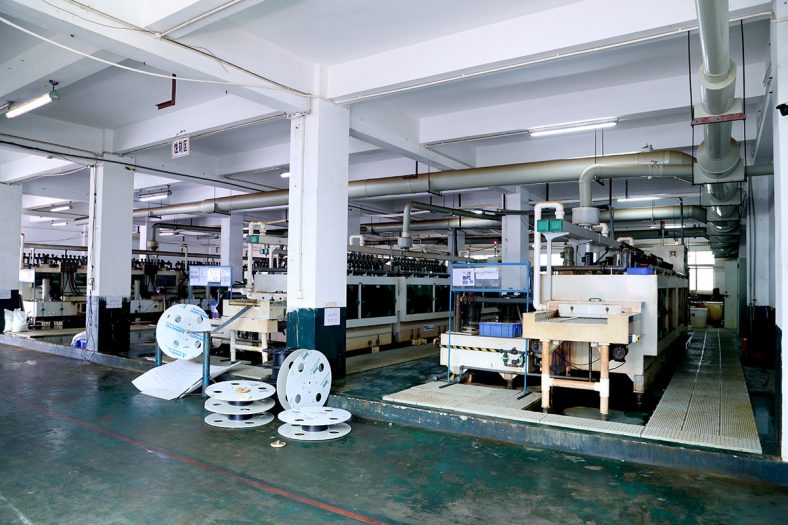
We are committed to enlisting the full support of all employees to continuously improve our processes and enhance quality, thereby fulfilling our customer's needs with defect free products and services, on time and every time
- ISO 9001:2015 certified
- Compliance in DFARS materials sourcing requirements
- Strict compliance with PPAP and Process FMEA
- Fully compliant with the exacting requirements of our customers
- ITAR registered
- NIST cybersecurity standard compliant
- Proprietary Patented quality systems
- Skilled in KanBan and other customer driven quality and inventory management systems
Metal Etching Material
BE-CU is experienced in precision etching various metals, allowing customers the freedom to specify components in hundreds of different materials.


The Surface Treatment Of Metal Etching Parts
Do you want your etching parts to be more corrosion-resistant or get a specific look? Metal finishing service is a essential choice to achieve your design perfectly. BE-CU – metal-etch.com is an accomplished finished parts manufacturer, our workers and craftsman are capable to provide precision metal etching services and a wide range of finishing services including aluminum anodizing, painting, passivation, electroplating, powder coating, polishing, black oxide, conversion coating, abrasive blasting, etc. We offers several common surface finishes to help improve functionality and aesthetics.
- Anodizing (Anodized)
- Passivation
- Plating (Electroplating)
- Painting
- Black Oxide (Hot Blackening)
- Polishing
- Powder Coating
- Heat Treatment
- Satin Finish
- Abrasive blasting (Sandblasting)
- Conversion coating
- Tungsten carbide coating
After browsing a list of metal finishing services, select a process based on essential considerations, like production time, cost-effectiveness, part tolerance, durability and applications. High-tolerance metal etching parts are not recommended to apply secondary metal surface finish, because the treatment may change the sizes of the finished part through removing or adding a small amount of materials.
Other requirements or custom designs, welcome to contact us for a free quote fast!
