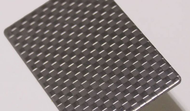
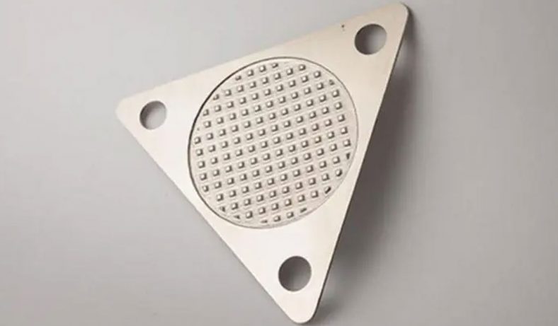
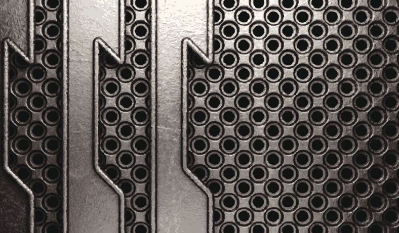
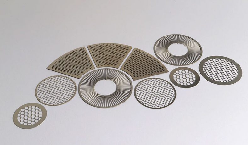
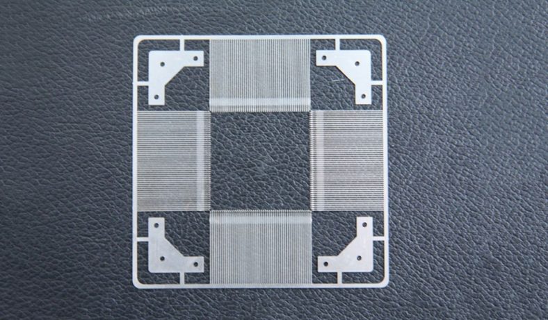
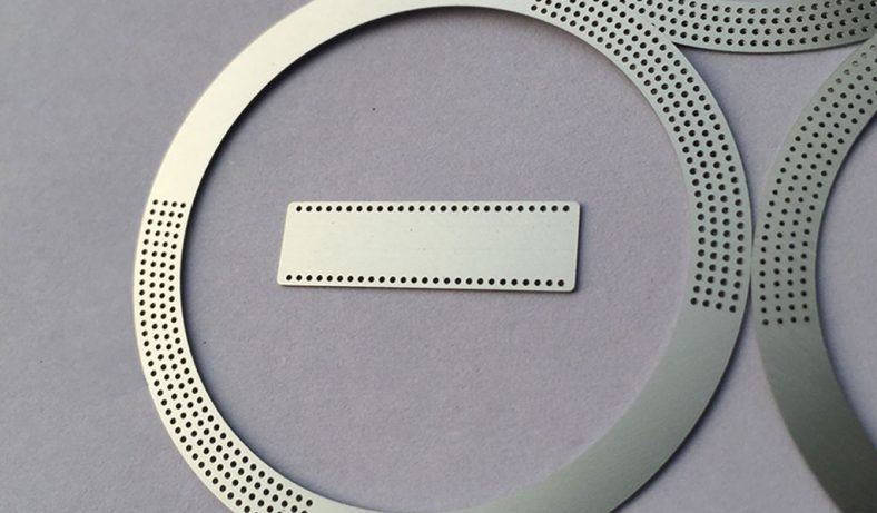
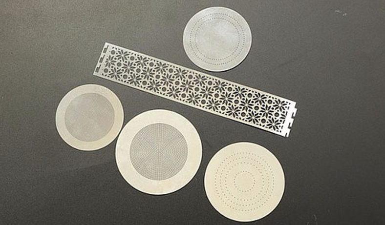
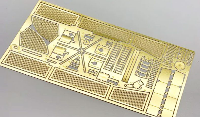
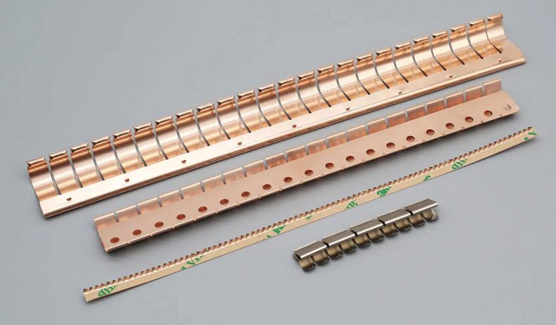
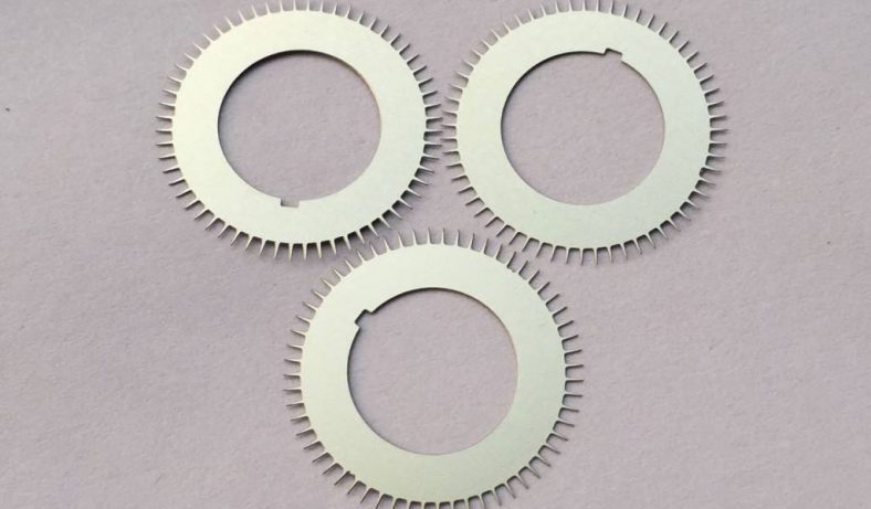
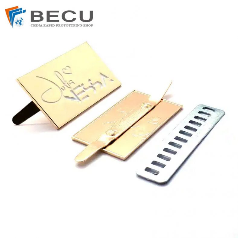
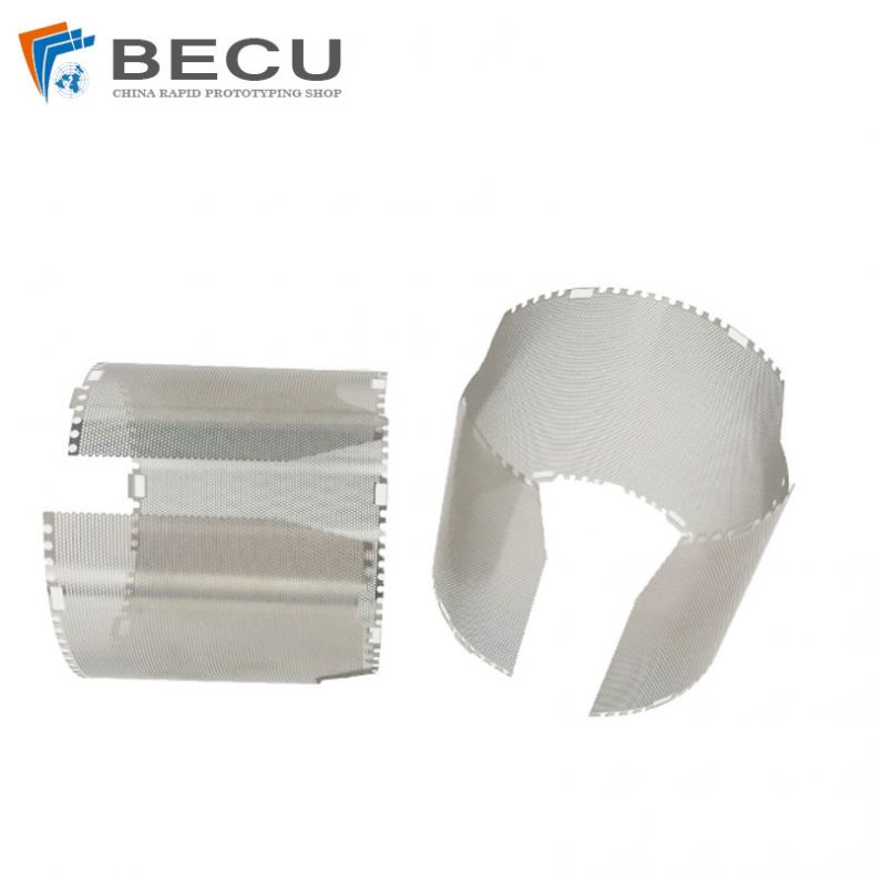
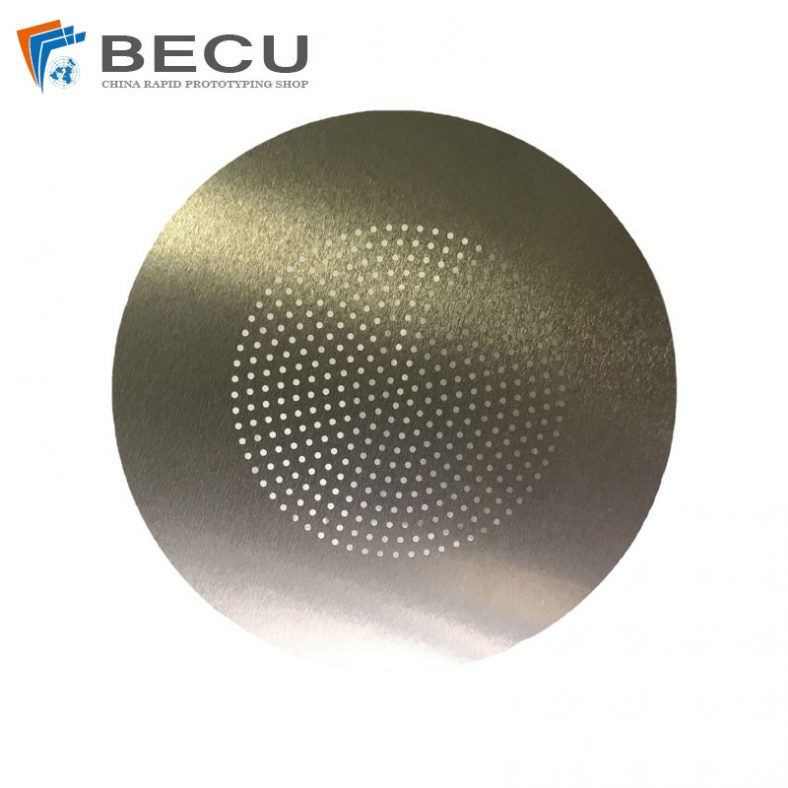
Electromagnetic compatibility (EMC) shielding plays a critical role in protecting electronic devices from electromagnetic interference (EMI), ensuring their reliable operation across various industries. Etching is a widely utilized manufacturing method for producing intricate and highly precise shielding components. This article delves deeply into the process, materials, applications, and advantages of etching EMC shielding, highlighting its importance in modern electronics.
Overview of EMC Shielding
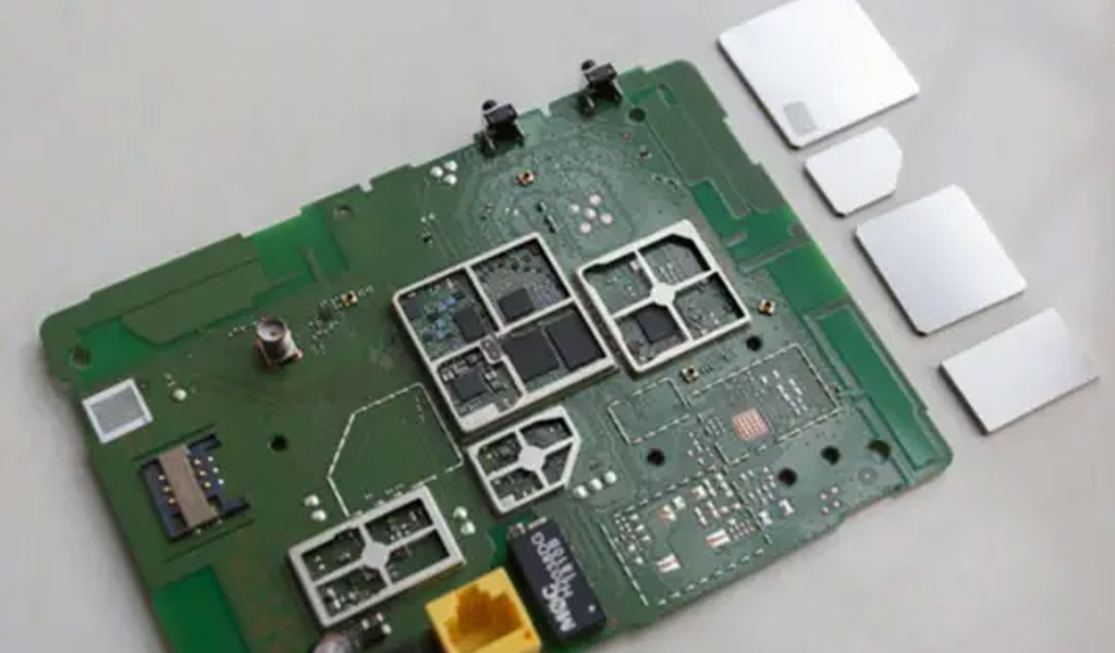
EMC shielding is designed to reduce or block electromagnetic waves from affecting sensitive electronic components. It achieves this by enclosing the components within conductive materials that reflect, absorb, or redirect electromagnetic waves.
Effective EMC shielding is crucial in environments with high electromagnetic activity, such as automotive systems, medical devices, aerospace equipment, and consumer electronics.
The demand for precise and lightweight shielding components has led to the adoption of advanced manufacturing techniques. Among these, chemical etching has emerged as a leading choice due to its ability to produce intricate designs with high accuracy and repeatability.
Fundamentals of Etching in Manufacturing
Etching is a subtractive manufacturing process that removes material from a workpiece to create specific patterns or designs. It is a non-contact method that employs chemical solutions, photolithography, or other processes to achieve desired results. The etched parts are characterized by high precision, smooth edges, and the ability to incorporate complex geometries.
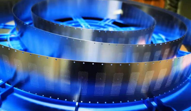
Chemical etching, the most common method for producing EMC shielding, involves the application of a protective resist on the metal surface. The resist masks specific areas of the material, exposing the unmasked sections to chemical solutions that dissolve the material. This enables the creation of fine details and consistent results, even for high-volume production runs.
Steps in Etching EMC Shielding
The etching process for EMC shielding components involves several critical stages to ensure precision and reliability. Each step must be meticulously controlled to achieve the desired results.
- Material Selection
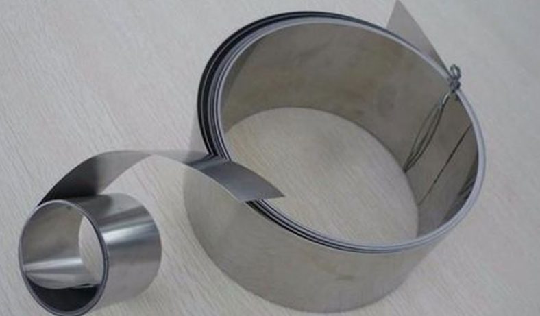
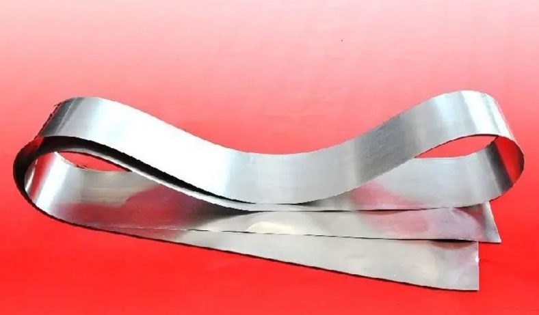
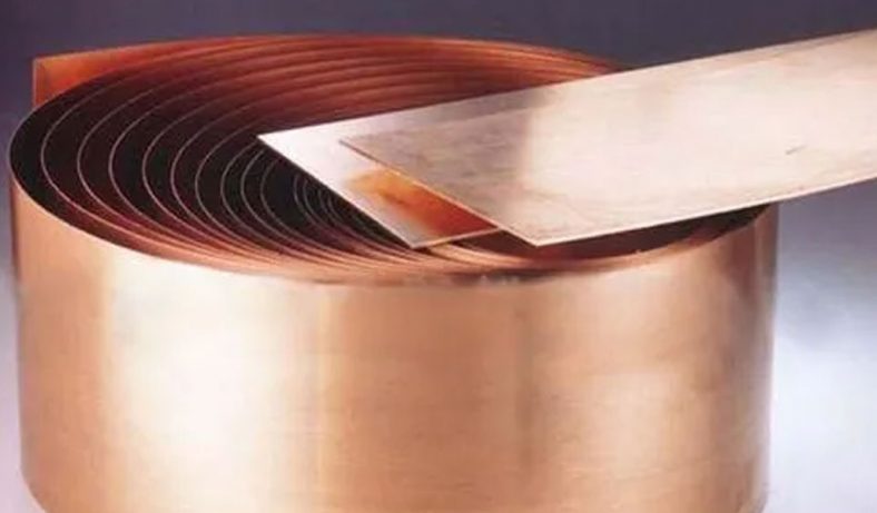
- The choice of material significantly influences the performance of EMC shielding. Common materials include copper, brass, aluminum, stainless steel, and nickel alloys. These materials offer high conductivity and excellent EMI attenuation properties.
- Factors such as thickness, conductivity, corrosion resistance, and mechanical properties are considered when selecting the material.
- Design Preparation
- The shielding design is typically created using computer-aided design (CAD) software. This allows for the incorporation of intricate patterns, perforations, and other features necessary for specific applications.
- The design is converted into a photomask or stencil that will guide the etching process.
- Surface Cleaning
- The material surface is thoroughly cleaned to remove contaminants, such as oils, dirt, or oxides. Cleaning ensures proper adhesion of the photoresist and enhances the overall quality of the etching.
- Photoresist Application
- A layer of photoresist, a light-sensitive material, is applied to the cleaned metal surface. This can be done through dipping, spraying, or laminating.
- The photoresist acts as a protective barrier, shielding specific areas of the metal during the etching process.
- UV Exposure and Development
- The photoresist-coated material is exposed to ultraviolet (UV) light through the photomask. The exposed areas of the photoresist harden, while the unexposed sections remain soft.
- The soft photoresist is subsequently removed using a developer solution, revealing the underlying metal for etching.
- Chemical Etching
- The prepared material is immersed in a chemical etchant, such as ferric chloride, nitric acid, or cupric chloride. The etchant reacts with the exposed metal, dissolving it to create the desired pattern.
- The etching duration, temperature, and solution concentration are carefully controlled to ensure uniformity and precision.
- Photoresist Stripping
- After etching, the remaining photoresist is stripped away using a suitable solvent or chemical solution. This step reveals the final etched pattern.
- Post-Etching Treatment
- The etched components undergo cleaning to remove any residual chemicals. Additional treatments, such as passivation or coating, may be applied to enhance corrosion resistance or aesthetic appeal.
- Quality Inspection
- The etched components are inspected for accuracy, edge quality, and compliance with design specifications. Non-destructive testing methods, such as optical inspection or X-ray fluorescence, are used to verify the quality.
Advantages of Etching for EMC Shielding
The etching process offers numerous advantages, making it an ideal choice for producing EMC shielding components:
- High Precision: Etching enables the production of intricate designs with tight tolerances, ensuring optimal performance.
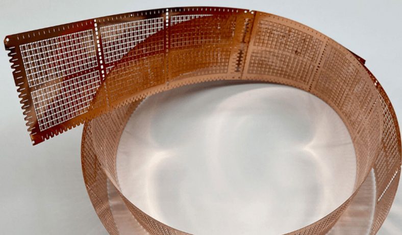
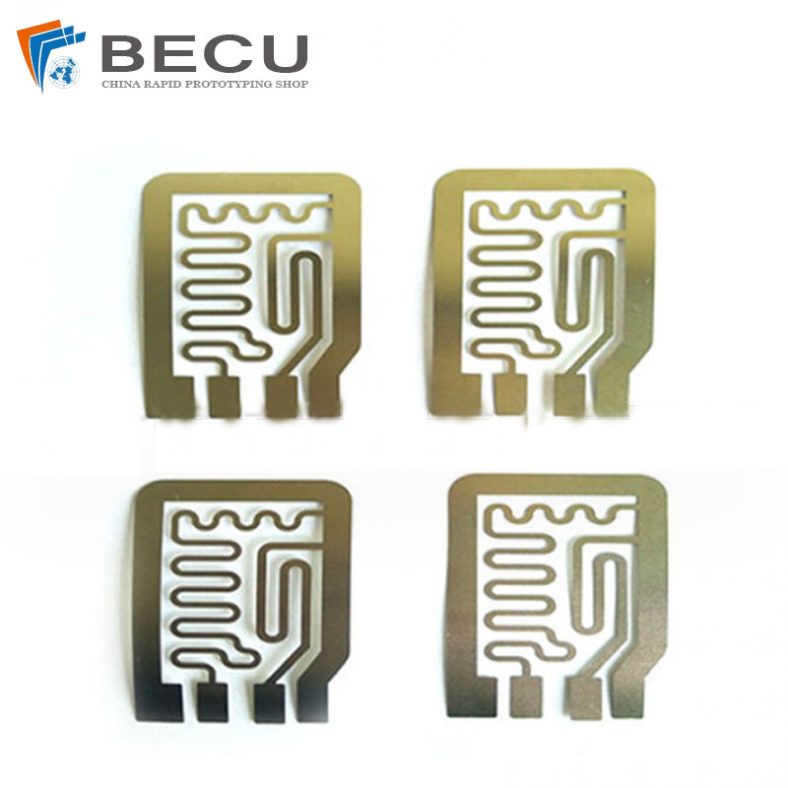
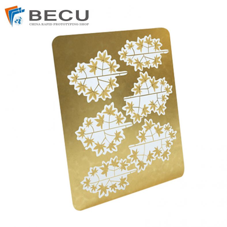
- Design Flexibility: Complex geometries, perforations, and logos can be incorporated without additional tooling costs.
- Material Efficiency: Unlike machining or stamping, etching minimizes material wastage, making it a cost-effective option.
- Scalability: Etching is suitable for both prototyping and high-volume production, allowing manufacturers to scale operations as needed.
- Non-Contact Process: The absence of physical contact eliminates the risk of mechanical stress or deformation in delicate components.
Applications of Etched EMC Shielding
Etched EMC shielding is employed across diverse industries to address specific electromagnetic compatibility challenges:
- Consumer Electronics: Protects smartphones, laptops, and tablets from external EMI, ensuring uninterrupted performance.
- Automotive Systems: Shields electronic control units (ECUs), sensors, and infotainment systems from interference in high-EMI environments.
- Aerospace and Defense: Ensures the reliability of avionics, communication systems, and radar equipment.
- Medical Devices: Safeguards sensitive instruments, such as pacemakers and imaging systems, from electromagnetic interference.
- Telecommunications: Enhances the performance of antennas, base stations, and signal amplifiers by minimizing signal disruptions.
Emerging Trends in Etching EMC Shielding
As electronics become more compact and sophisticated, the demand for advanced EMC shielding solutions continues to grow. Several trends are shaping the future of etched shielding:
- Miniaturization: The push for smaller devices requires thinner and more intricate shielding components, driving innovation in etching techniques.
- Sustainable Practices: Manufacturers are adopting eco-friendly etchants and recycling processes to reduce environmental impact.
- Advanced Materials: The development of composite materials and multilayer shielding structures expands the capabilities of etched components.
- Automation and AI: The integration of automation and artificial intelligence enhances the efficiency and accuracy of etching processes.
Conclusion
Etching has revolutionized the production of EMC shielding components, offering unmatched precision, flexibility, and scalability. Its ability to create intricate designs while maintaining material integrity makes it indispensable in modern manufacturing. As technology advances, etching will continue to evolve, addressing emerging challenges and meeting the demands of increasingly complex electronic systems. By understanding the intricacies of this process, manufacturers can leverage its benefits to produce high-quality shielding solutions for a wide range of applications.

