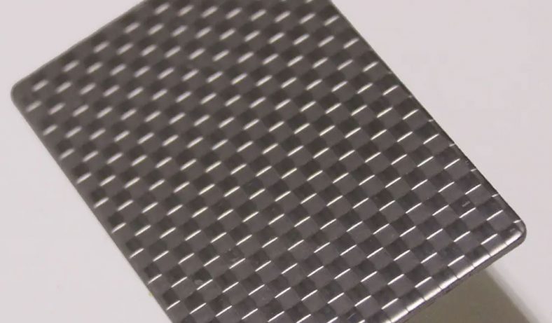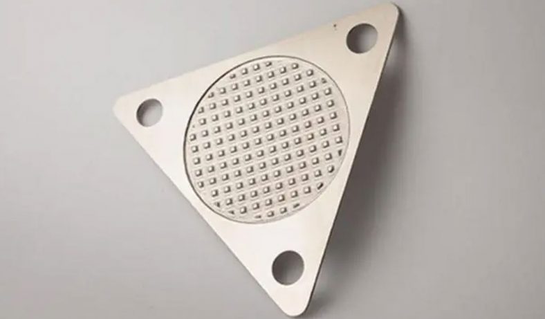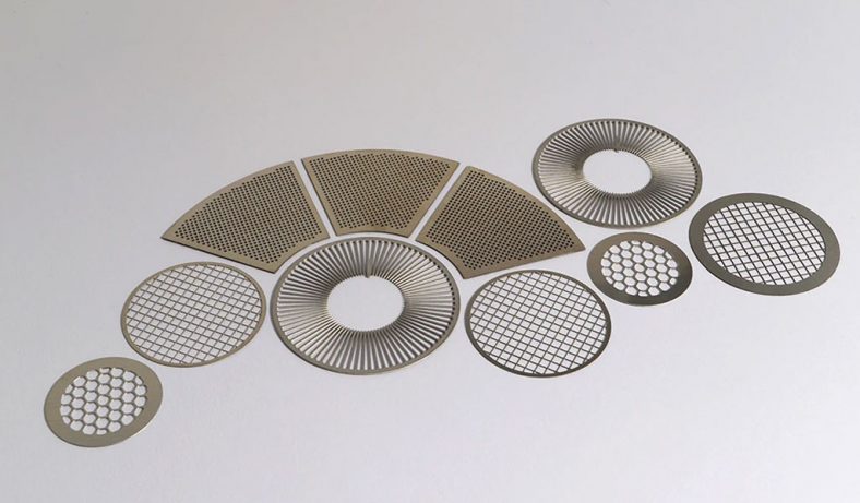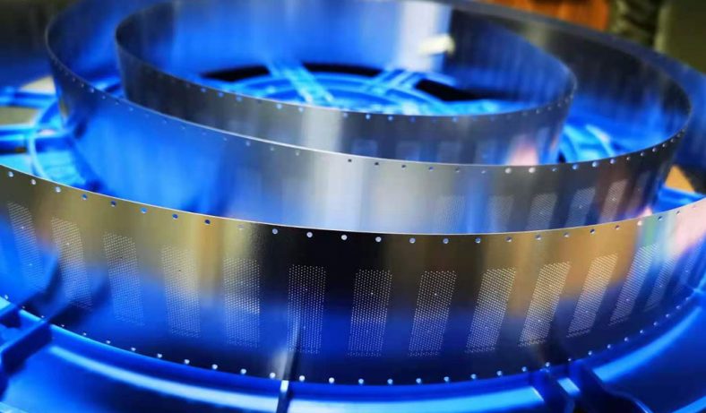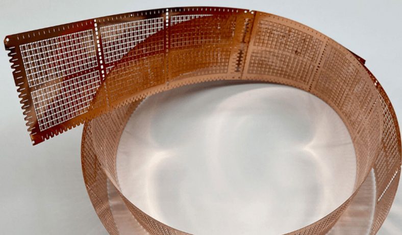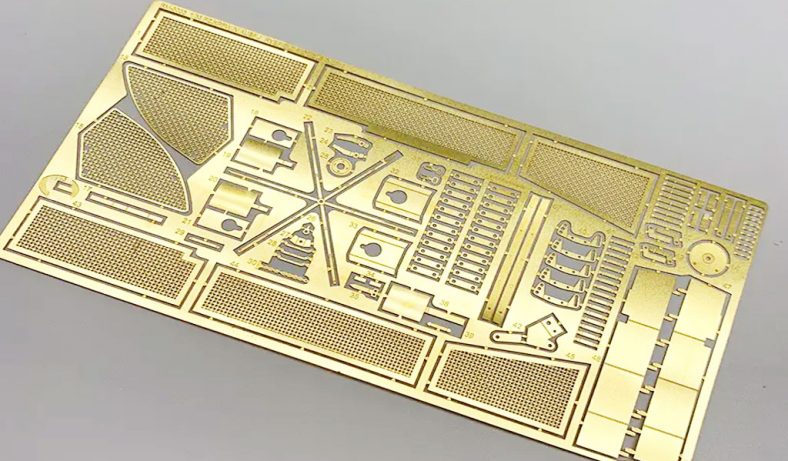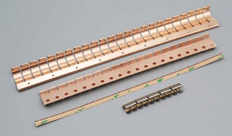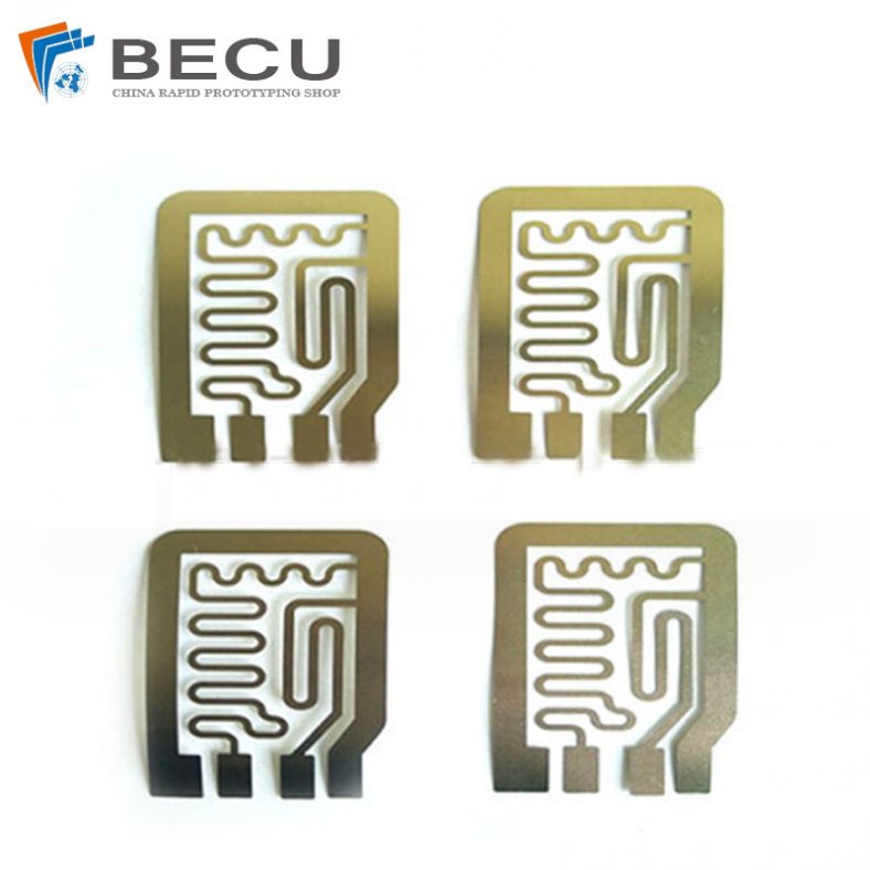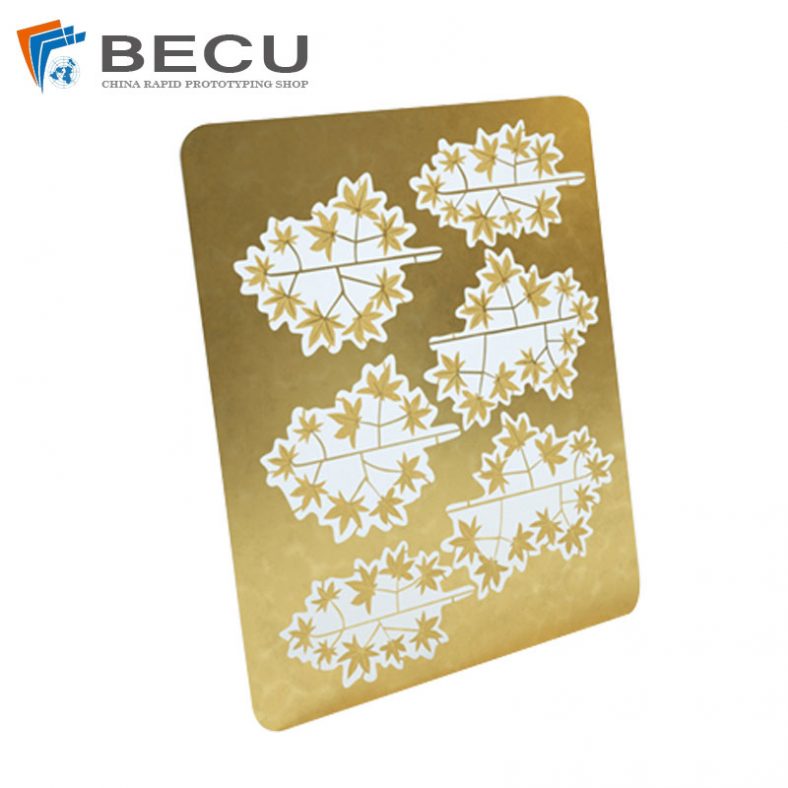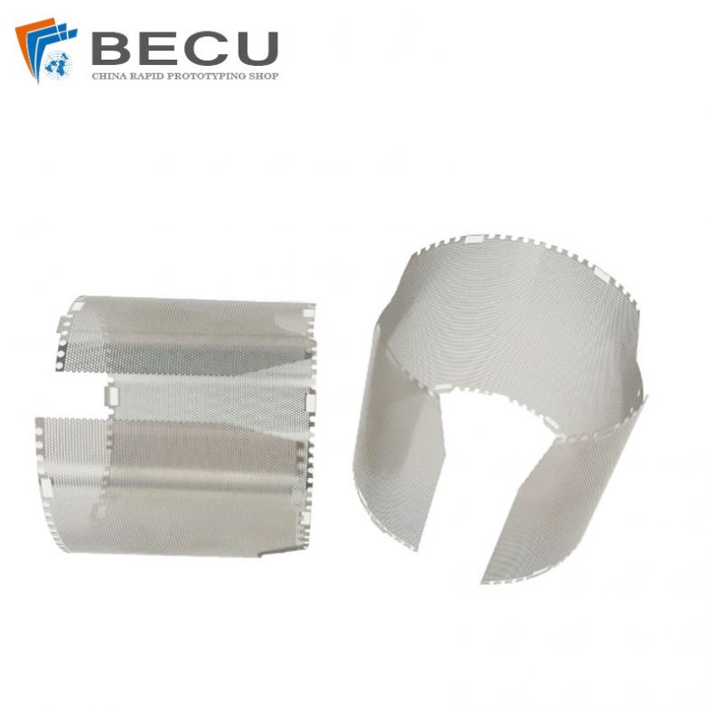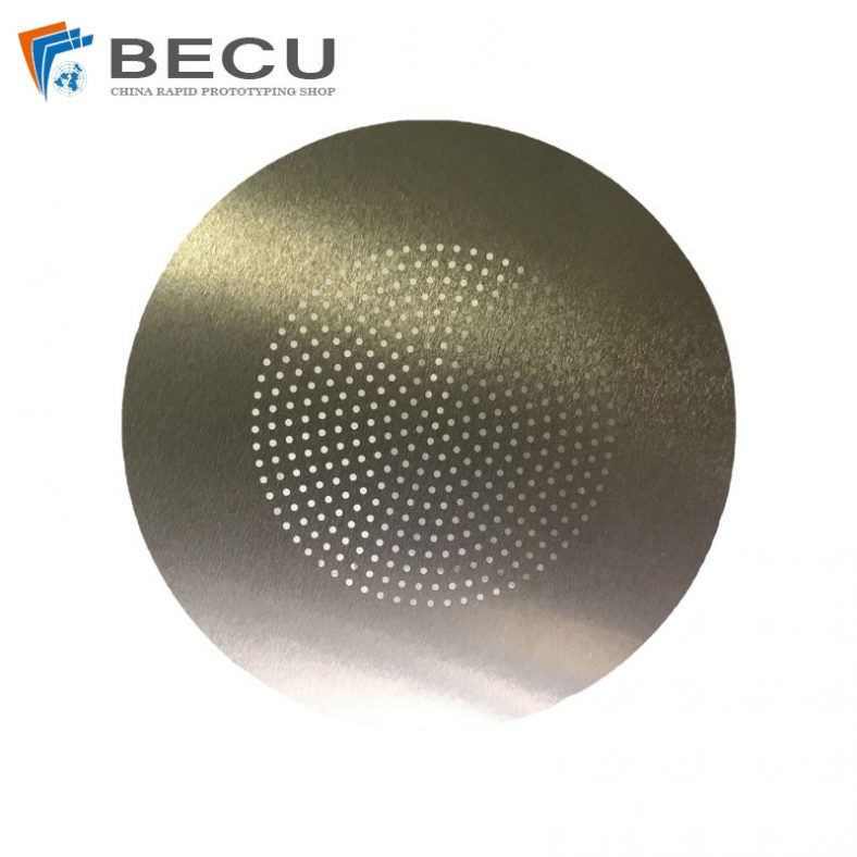
Etching is a critical process in the fabrication of semiconductor devices and integrated circuits. It involves the selective removal of material from a substrate to create patterns and structures necessary for the functioning of electronic components.
In the context of laminated films, particularly those including reflective electrodes, etching plays a pivotal role in defining the precise geometries required for optimal performance. This article delves into the composition of etching solutions used for laminated films with reflective electrodes and the methods for forming laminated wiring structures.
Etching Composition
The composition of the etching solution is crucial for achieving high-quality etching results. The primary components of an etching solution include acids, oxidizing agents, and sometimes surfactants. The choice of these components depends on the material being etched and the desired etching rate and selectivity.
Acids
Acids are the primary etching agents in most solutions. Common acids used in etching compositions include:
- Hydrofluoric Acid (HF): Often used for etching silicon dioxide (SiO2) and other oxides. It is highly corrosive and must be handled with extreme care.
- Nitric Acid (HNO3): Used for etching metals such as copper and aluminum. It is a strong oxidizing agent.
- Phosphoric Acid (H3PO4): Used for etching aluminum and other metals. It is less corrosive than HF and HNO3.
- Sulfuric Acid (H2SO4): Often used in combination with other acids for etching metals and semiconductors.
Oxidizing Agents
Oxidizing agents enhance the etching rate by promoting the oxidation of the material being etched. Common oxidizing agents include:
- Hydrogen Peroxide (H2O2): Often used in combination with acids to enhance etching rates.
- Potassium Permanganate (KMnO4): A strong oxidizing agent used in various etching solutions.
- Chromic Acid (H2CrO4): Used for etching metals and semiconductors. It is highly corrosive and toxic.
Surfactants
Surfactants are added to etching solutions to improve wetting and reduce surface tension. This helps in achieving uniform etching and preventing the formation of defects. Common surfactants include:
- Sodium Dodecyl Sulfate (SDS): A widely used anionic surfactant.
- Triton X-100: A non-ionic surfactant used in various etching solutions.
Comparison of Etching Solutions
The following table compares different etching solutions based on their composition, etching rate, and selectivity:
| Etching Solution | Composition | Etching Rate | Selectivity |
|---|---|---|---|
| HF Solution | HF, H2O | High | SiO2 |
| Nitric Acid Solution | HNO3, H2O | Moderate | Copper, Aluminum |
| Phosphoric Acid Solution | H3PO4, H2O | Moderate | Aluminum |
| Sulfuric Acid Solution | H2SO4, H2O | High | Metals, Semiconductors |
| HF-HNO3 Solution | HF, HNO3, H2O | High | SiO2, Metals |
| H2O2-H2SO4 Solution | H2O2, H2SO4, H2O | High | Metals, Semiconductors |
Methods for Forming Laminated Wiring Structures
The formation of laminated wiring structures involves several steps, including deposition, patterning, and etching. The following sections describe these steps in detail.
Deposition
Deposition is the process of applying a thin film of material onto a substrate. Common deposition techniques include:
- Chemical Vapor Deposition (CVD): Involves the reaction of gaseous precursors to form a thin film on the substrate.
- Physical Vapor Deposition (PVD): Involves the physical transfer of material from a source to the substrate, typically using techniques such as sputtering or evaporation.
- Electroplating: Involves the deposition of a metal layer onto a conductive substrate using an electric current.
Patterning
Patterning is the process of creating a desired pattern on the deposited film. This is typically achieved using photolithography, which involves the following steps:
- Photoresist Coating: A layer of photoresist is applied to the substrate.
- Exposure: The photoresist is exposed to UV light through a photomask, which defines the desired pattern.
- Development: The exposed photoresist is developed, removing the unexposed areas and leaving the desired pattern.
Etching
Etching is the process of selectively removing material from the substrate to create the desired pattern. The choice of etching technique depends on the material being etched and the desired etching rate and selectivity. Common etching techniques include:
- Wet Etching: Involves the use of liquid etching solutions to remove material. Wet etching is isotropic, meaning it etches in all directions.
- Dry Etching: Involves the use of gaseous etching agents to remove material. Dry etching is anisotropic, meaning it etches primarily in the vertical direction.
Comparison of Etching Techniques
The following table compares different etching techniques based on their etching rate, selectivity, and anisotropy:
| Etching Technique | Etching Rate | Selectivity | Anisotropy |
|---|---|---|---|
| Wet Etching | Moderate | High | Isotropic |
| Dry Etching | High | High | Anisotropic |
Reflective Electrode Formation
Reflective electrodes are crucial for enhancing the optical properties of laminated films. The formation of reflective electrodes involves the deposition of reflective materials such as aluminum, silver, or gold. The following steps are typically involved:
- Deposition: The reflective material is deposited onto the substrate using techniques such as PVD or electroplating.
- Patterning: The reflective material is patterned using photolithography to define the electrode geometry.
- Etching: The patterned reflective material is etched to create the final electrode structure.
Comparison of Reflective Materials
The following table compares different reflective materials based on their optical properties and etching characteristics:
| Reflective Material | Optical Properties | Etching Characteristics |
|---|---|---|
| Aluminum | High reflectivity | Easy to etch |
| Silver | High reflectivity | Moderate etching difficulty |
| Gold | High reflectivity | Difficult to etch |
Applications
The etching composition and methods for forming laminated wiring structures have numerous applications in the semiconductor industry. Some of the key applications include:
- Integrated Circuits (ICs): Etching is used to create the intricate patterns and structures required for ICs.
- Microelectromechanical Systems (MEMS): Etching is used to create the microscale structures and devices in MEMS.
- Optoelectronics: Etching is used to create the precise geometries required for optoelectronic devices such as LEDs and solar cells.
- Sensors: Etching is used to create the sensitive elements and structures in sensors.
Challenges and Future Directions
Despite the advancements in etching compositions and methods, several challenges remain. These include:
- Selectivity: Achieving high selectivity between different materials is a ongoing challenge.
- Uniformity: Ensuring uniform etching across the substrate is crucial for high-quality devices.
- Environmental Impact: The use of hazardous chemicals in etching solutions poses environmental and health risks.
Future research is focused on addressing these challenges through the development of new etching compositions and techniques. Some of the emerging trends include:
- Green Etching: The development of environmentally friendly etching solutions that minimize the use of hazardous chemicals.
- Nanoscale Etching: The development of etching techniques capable of creating nanoscale structures and patterns.
- Automated Etching: The use of automated systems to improve the precision and uniformity of etching processes.
Conclusion
Etching is a fundamental process in the fabrication of semiconductor devices and integrated circuits. The composition of etching solutions and the methods for forming laminated wiring structures play a critical role in defining the precise geometries required for optimal performance. Advances in etching compositions and techniques continue to drive innovation in the semiconductor industry, enabling the development of increasingly complex and high-performance devices. As research continues, the focus will be on addressing the challenges of selectivity, uniformity, and environmental impact, paving the way for the next generation of semiconductor technologies.

