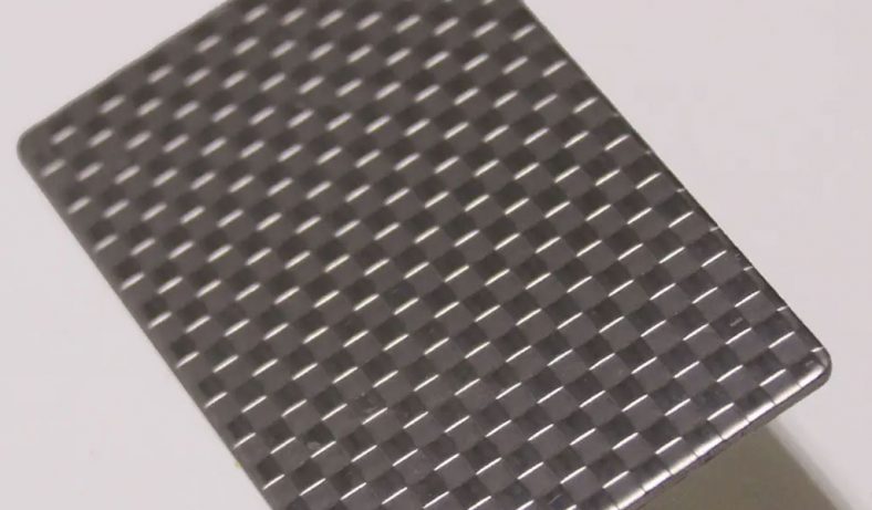
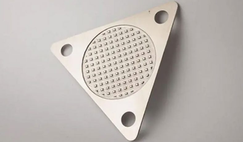
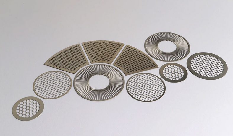
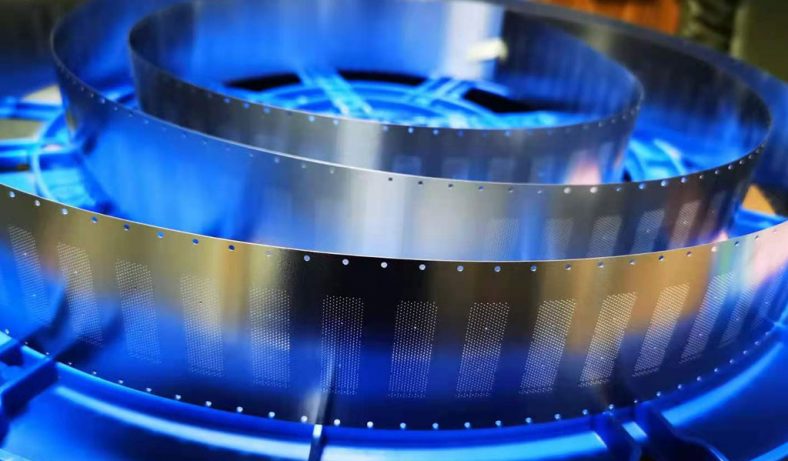
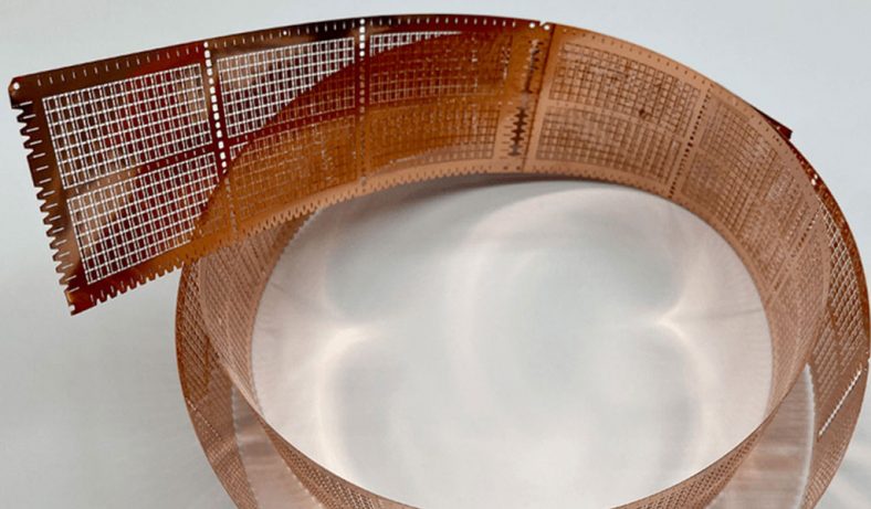
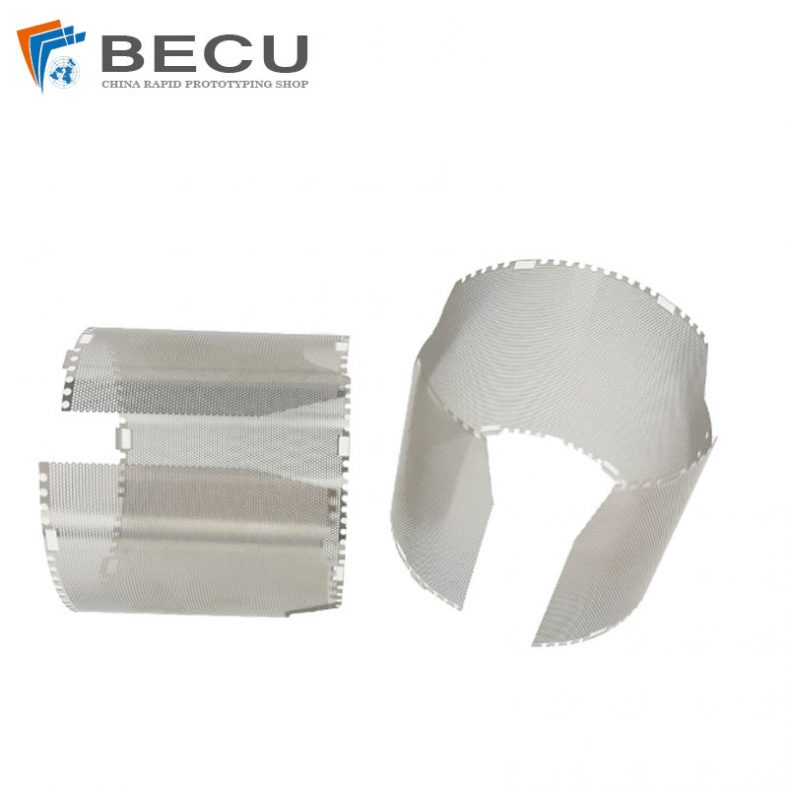
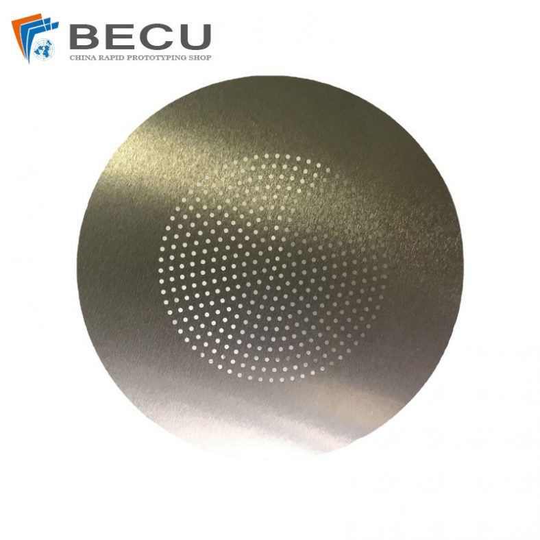
Metal etching is a critical process in the fabrication of microelectronic devices, printed circuit boards (PCBs), and advanced semiconductor packaging. It involves the selective removal of metal layers from a substrate to create intricate patterns that form the basis of electronic circuits and microstructures. Central to this process is the use of a mask—typically a photoresist or hard mask—that protects certain areas of the metal while exposing others to the etching agent. Once the etching is complete, the mask must be removed in a process known as mask stripping. This step is vital to ensure the integrity of the etched features and to prepare the substrate for subsequent manufacturing stages.
In recent decades, the demand for smaller, more complex, and higher-performance electronic devices has driven significant advancements in etching and mask stripping technologies. Automation has emerged as a transformative force in this domain, enabling higher precision, repeatability, and throughput while reducing human error and operational costs. This article explores the automation research surrounding mask stripping technology in metal etching, covering its historical evolution, current methodologies, technological innovations, and future directions. Detailed comparisons of various techniques and their performance metrics are provided to offer a comprehensive understanding of the field.
Historical Context of Mask Stripping in Metal Etching
Early Methods of Mask Stripping
The origins of metal etching and mask stripping can be traced back to the early days of microelectronics in the mid-20th century. During this period, wet chemical etching was the dominant method for patterning metal layers on substrates. Photoresists, typically organic polymers sensitive to light, were applied to the metal surface and patterned using photolithography. After etching, the photoresist was removed using simple solvent-based solutions, such as acetone or alcohol, in manual or semi-automated processes.
These early methods were effective for the relatively large feature sizes of the time (on the order of micrometers). However, they were labor-intensive, prone to variability, and limited in their ability to handle complex patterns. The stripping process often required prolonged immersion in chemical baths, which could damage the underlying metal or substrate if not carefully controlled. Moreover, the isotropic nature of wet etching led to undercutting of the mask, reducing pattern fidelity and necessitating more robust stripping techniques.
Transition to Dry Etching and Plasma Stripping
The advent of very-large-scale integration (VLSI) and ultra-large-scale integration (ULSI) in the 1970s and 1980s marked a significant shift in etching technology. Wet etching was largely supplanted by dry etching methods, such as reactive ion etching (RIE) and inductively coupled plasma (ICP) etching, which offered greater anisotropy and precision for sub-micrometer features. These methods required more resilient masks, including hard masks made of materials like silicon dioxide (SiO₂), silicon nitride (Si₃N₄), or metals such as chromium (Cr) and titanium (Ti).
The shift to dry etching necessitated corresponding advancements in mask stripping. Plasma-based stripping, using oxygen (O₂) or fluorine-based gases (e.g., CF₄, SF₆), emerged as a preferred method for removing organic photoresists and certain hard masks. Plasma stripping offered several advantages, including faster processing times, reduced chemical waste, and compatibility with automated systems. However, it also introduced challenges, such as potential damage to the substrate from ion bombardment and the need for precise control of plasma parameters.
Emergence of Automation in Semiconductor Manufacturing
The 1980s saw the rise of automation in semiconductor manufacturing, driven by the need for higher throughput and consistency in high-volume production environments. Early automated systems focused on wafer handling, chemical dispensing, and process monitoring. In the context of mask stripping, automation enabled the integration of stripping processes into cassette-to-cassette workflows, where wafers were automatically transferred between etching, stripping, and cleaning stations.
These systems relied on programmable logic controllers (PLCs) and rudimentary robotics to manage process sequences. While effective for the time, they lacked the sophistication needed to address the increasing complexity of modern semiconductor devices, particularly as feature sizes shrank below 100 nanometers and new materials were introduced.
Fundamentals of Mask Stripping in Metal Etching
Role of Masks in Metal Etching
Masks serve as temporary protective layers during metal etching, defining the areas where material is to be removed or preserved. The choice of mask material depends on the etching chemistry, the metal being etched, and the desired feature size. Common mask types include:
- Photoresists: Organic polymers (e.g., positive or negative resists) patterned via photolithography. They are widely used for their ease of application and removal but are less durable under aggressive etching conditions.
- Hard Masks: Inorganic materials like SiO₂, Si₃N₄, or metals (e.g., Cr, Ti, Ni). These are more resistant to plasma etching but often require specialized stripping processes.
- Metal Masks: Thin films of metals like gold (Au), aluminum (Al), or titanium (Ti) used in specific applications, such as deep diamond etching or metal-assisted chemical etching (MACE).
The stripping process must remove the mask completely without damaging the underlying metal or substrate, which may include delicate features or sensitive materials.
Challenges in Mask Stripping
Mask stripping presents several challenges, particularly in automated systems:
- Selectivity: The stripping process must target the mask material without affecting the etched metal or substrate. For example, stripping a photoresist from a copper (Cu) surface requires chemistries that do not corrode or oxidize the copper.
- Residue Removal: Etching and stripping processes can leave residues, such as polymerized photoresist or redeposited metal, which must be thoroughly removed to prevent defects.
- Compatibility: The stripping method must be compatible with the materials and structures on the wafer, including dielectrics, semiconductors, and interconnects.
- Throughput: High-volume manufacturing demands fast stripping processes to maintain production efficiency.
- Environmental Impact: Traditional wet stripping methods generate significant chemical waste, prompting research into greener alternatives.
Automation addresses these challenges by enabling precise control of process parameters, real-time monitoring, and integration with other fabrication steps.
Common Mask Stripping Techniques
Mask stripping techniques can be broadly categorized into wet and dry methods, each with distinct advantages and limitations.
Wet Stripping
Wet stripping involves immersing the substrate in a chemical solution that dissolves or lifts off the mask. Common wet stripping chemistries include:
- Solvent-Based Strippers: Organic solvents like N-methyl-2-pyrrolidone (NMP) or dimethyl sulfoxide (DMSO) for photoresist removal. These are effective for organic masks but may require heating or agitation.
- Alkaline Strippers: Solutions like tetramethylammonium hydroxide (TMAH) or potassium hydroxide (KOH) for removing photoresists and certain hard masks. These are often used in high-speed horizontal processing lines.
- Acidic Strippers: Nitric acid or hydrofluoric acid-based solutions for metal masks or inorganic hard masks. These require careful handling due to their corrosive nature.
Wet stripping is cost-effective and widely used in PCB manufacturing and less critical applications. However, it is isotropic, leading to potential undercutting, and generates significant waste, posing environmental challenges.
Dry Stripping
Dry stripping, primarily plasma-based, uses reactive gases in a vacuum chamber to remove the mask. Key methods include:
- Oxygen Plasma Stripping: Uses O₂ plasma to ash organic photoresists, converting them into volatile compounds like CO₂ and H₂O. This is highly effective for photoresist removal but may not work for inorganic masks.
- Fluorine-Based Plasma Stripping: Employs gases like CF₄ or SF₆ to remove SiO₂ or Si₃N₄ hard masks. These are selective but can damage sensitive substrates if not carefully controlled.
- Chlorine-Based Plasma Stripping: Uses gases like BCl₃ or Cl₂ for metal masks, such as Al or Cr. These offer high selectivity but require specialized equipment.
Dry stripping is anisotropic, enabling precise control over feature dimensions, and produces less waste than wet methods. However, it requires expensive equipment and careful optimization to avoid substrate damage.
Automation in Mask Stripping: Technological Foundations
Evolution of Automation Systems
Automation in mask stripping has evolved alongside broader trends in semiconductor manufacturing. Early automation systems in the 1980s and 1990s focused on mechanizing repetitive tasks, such as wafer loading and unloading, using robotic arms and conveyor systems. These systems were controlled by PLCs and relied on pre-programmed sequences, offering limited flexibility.
The introduction of computer numerical control (CNC) and advanced robotics in the 2000s enabled more sophisticated automation. Modern systems integrate sensors, machine vision, and real-time feedback loops to monitor and adjust process parameters dynamically. These advancements have been critical for mask stripping, where precision and repeatability are paramount.
Key Components of Automated Mask Stripping Systems
Automated mask stripping systems typically include the following components:
- Robotic Wafer Handling: Robots transfer wafers between process chambers, ensuring contamination-free handling. Systems like those from Brooks Automation can handle 300 mm wafers with sub-micrometer precision.
- Process Chambers: Dedicated chambers for wet or dry stripping, equipped with precise control over temperature, pressure, gas flow, and plasma power. For example, Lam Research’s plasma stripping tools use advanced RF generators for stable plasma conditions.
- Chemical Delivery Systems: Automated pumps and valves dispense precise volumes of stripping chemicals, minimizing waste and ensuring consistency. Technic Inc.’s TechniStrip systems are examples of automated wet stripping solutions.
- Sensors and Metrology: In-line sensors monitor parameters like etch rate, residue levels, and surface cleanliness. Optical emission spectroscopy (OES) and residual gas analysis (RGA) are commonly used in plasma stripping.
- Control Software: Software platforms, such as Applied Materials’ APF (Advanced Productivity Family), integrate process control, data logging, and fault detection, enabling real-time optimization.
Role of Artificial Intelligence and Machine Learning
Recent advancements in artificial intelligence (AI) and machine learning (ML) have revolutionized automation in mask stripping. AI algorithms analyze data from sensors and metrology tools to predict process outcomes and optimize parameters. For example, ML models can adjust plasma power and gas flow in real-time to minimize residue formation or substrate damage.
AI also enables predictive maintenance, identifying potential equipment failures before they occur. Companies like Tokyo Electron have implemented AI-driven systems that reduce downtime by up to 30% in etching and stripping processes. Furthermore, ML techniques are used to develop digital twins—virtual models of stripping systems—that simulate process behavior and guide optimization.
Current Research in Automated Mask Stripping
Wet Stripping Automation
Advances in Chemical Formulations
Research in wet stripping automation focuses on developing high-performance chemistries that are compatible with automated systems. For instance, Technic Inc.’s TechniStrip NF52 is an NMP-free photoresist remover designed for through-silicon via (TSV) and solder bumping applications. It offers high dissolution rates and compatibility with metals like Cu and Al, making it suitable for automated high-throughput lines.
Other innovations include fluoride-free strippers, such as TechniEtch TBR19, which selectively dissolve titanium-based barriers without damaging copper interconnects. These chemistries are integrated into automated spray or immersion systems, where precise control over temperature and agitation ensures uniform stripping.
Automated Wet Stripping Equipment
Modern wet stripping equipment features advanced automation capabilities. For example, SUSS MicroTec’s ACS300 Gen2 system uses automated chemical delivery and real-time monitoring to process 300 mm wafers with minimal operator intervention. These systems incorporate features like:
- Closed-Loop Chemical Recycling: Reduces waste by filtering and reusing stripping solutions.
- In-Line Metrology: Uses optical inspection to detect residual photoresist or defects.
- Modular Design: Allows integration with etching and cleaning modules for seamless workflows.
Research is also exploring greener alternatives, such as water-based strippers and biodegradable solvents, to address environmental concerns. Automated systems are designed to handle these chemistries with minimal modifications, enhancing their adoption in sustainable manufacturing.
Dry Stripping Automation
Plasma Stripping Innovations
Plasma stripping is the dominant method for mask removal in advanced semiconductor fabrication, and automation has significantly enhanced its performance. Recent research focuses on improving selectivity, reducing substrate damage, and increasing throughput. Key innovations include:
- Pulsed Plasma Stripping: Alternates plasma on/off cycles to minimize ion bombardment and heat buildup. This technique, implemented in tools like Applied Materials’ Producer Etch, improves selectivity for delicate substrates.
- Low-Temperature Plasma: Uses cryogenic conditions to enhance anisotropy and reduce damage. Oxford Instruments’ PlasmaPro systems support low-temperature stripping for 2 nm node processes.
- Multi-Step Plasma Processes: Combine different gases (e.g., O₂ followed by CF₄) to remove complex mask stacks. Automated systems adjust gas ratios and RF power dynamically based on sensor feedback.
Automated Plasma Stripping Systems
Automated plasma stripping systems are designed for high-volume manufacturing. Lam Research’s Kiyo series, for example, integrates multiple process chambers with robotic wafer handling, achieving throughputs of over 100 wafers per hour. These systems use advanced control algorithms to maintain plasma uniformity across large wafers, critical for sub-5 nm nodes.
Research is also exploring the integration of extreme ultraviolet (EUV) lithography-compatible stripping systems. These systems, developed by companies like Tokyo Electron, use specialized plasma chemistries to remove EUV resists without damaging underlying layers. Automation ensures precise control over process parameters, minimizing variability in high-mix production environments.
Hybrid Stripping Approaches
Hybrid stripping, combining wet and dry methods, is an emerging area of research. For example, a process might use plasma stripping to remove the bulk of a photoresist, followed by a wet clean to eliminate residues. Automated systems like ASM’s Eagle platform support hybrid workflows, using integrated chambers for sequential processing.
Hybrid approaches offer several advantages:
- Improved Residue Removal: Wet cleaning enhances the removal of plasma-induced residues.
- Reduced Damage: Wet steps can be gentler on sensitive substrates compared to prolonged plasma exposure.
- Flexibility: Hybrid systems can handle a wide range of mask materials and substrates.
Research is focused on optimizing the transition between wet and dry steps, using automation to ensure seamless integration and minimal contamination.
Comparative Analysis of Mask Stripping Technologies
To provide a comprehensive understanding of automated mask stripping technologies, the following tables compare key methods based on performance metrics, applications, and limitations. These tables are derived from recent literature and industry data, ensuring relevance to current manufacturing practices.
Table 1: Comparison of Wet Stripping Technologies
| Parameter | Solvent-Based (e.g., NMP) | Alkaline (e.g., TMAH) | Acidic (e.g., Nitric Acid) |
|---|---|---|---|
| Selectivity | High for photoresists, low for metals | High for photoresists, moderate for Cu | High for metal masks, low for dielectrics |
| Residue Removal | Moderate, requires agitation | High, effective for polymerized resists | Moderate, may leave inorganic residues |
| Substrate Compatibility | Good for Cu, Al; poor for Ti | Good for Cu, Si; poor for Al | Good for Ti, Cr; poor for SiO₂ |
| Throughput | 50–100 wafers/hour | 100–150 wafers/hour | 30–80 wafers/hour |
| Environmental Impact | High (organic waste) | Moderate (alkaline waste) | High (acidic waste) |
| Automation Level | High (spray, immersion systems) | Very high (horizontal processing) | Moderate (batch processing) |
| Cost | Low | Moderate | High |
| Applications | PCB, MEMS | TSV, solder bumping | Hard mask removal, BEOL |
| Key Vendors | Technic Inc., DuPont | Technic Inc., BASF | Technic Inc., KMG Chemicals |
Notes:
- Throughput values assume 300 mm wafer processing.
- Environmental impact considers waste generation and disposal requirements.
- Automation level reflects the degree of integration with robotic handling and process control.
Table 2: Comparison of Dry Stripping Technologies
| Parameter | Oxygen Plasma | Fluorine-Based Plasma | Chlorine-Based Plasma |
|---|---|---|---|
| Selectivity | High for photoresists | High for SiO₂, Si₃N₄ | High for Al, Cr |
| Residue Removal | High, minimal residues | Moderate, may leave fluorocarbon residues | Moderate, requires post-clean |
| Substrate Compatibility | Good for Si, Cu; poor for organics | Good for Si, dielectrics; poor for metals | Good for metals; poor for SiO₂ |
| Throughput | 80–120 wafers/hour | 60–100 wafers/hour | 50–90 wafers/hour |
| Environmental Impact | Low (gas-based) | Moderate (fluorine emissions) | Moderate (chlorine emissions) |
| Automation Level | Very high (multi-chamber systems) | High (ICP, RIE systems) | High (parallel plate systems) |
| Cost | Moderate | High | High |
| Applications | Photoresist removal, FEOL | Hard mask removal, MEMS | Metal mask removal, BEOL |
| Key Vendors | Lam Research, Applied Materials | Tokyo Electron, Oxford Instruments | Plasma-Therm, SPTS Technologies |
Notes:
- Selectivity is relative to common substrates like Si, Cu, and Al.
- Throughput assumes single-wafer processing systems.
- Cost includes equipment and operational expenses.
Table 3: Comparison of Wet vs. Dry vs. Hybrid Stripping
| Parameter | Wet Stripping | Dry Stripping | Hybrid Stripping |
|---|---|---|---|
| Selectivity | Moderate to high | High | Very high |
| Residue Removal | Moderate | High | Very high |
| Substrate Compatibility | Variable, depends on chemistry | Good, with optimization | Excellent, combines benefits |
| Throughput | 30–150 wafers/hour | 50–120 wafers/hour | 40–100 wafers/hour |
| Environmental Impact | High | Low to moderate | Moderate |
| Automation Level | High | Very high | High |
| Cost | Low to moderate | High | Moderate to high |
| Applications | PCB, MEMS, TSV | FEOL, BEOL, advanced nodes | Complex stacks, EUV resists |
| Challenges | Waste management, undercutting | Substrate damage, equipment cost | Process integration, complexity |
Notes:
- Hybrid stripping throughput is lower due to sequential processing.
- Environmental impact for hybrid methods depends on the wet component’s chemistry.
Case Studies in Automated Mask Stripping
Case Study 1: TSMC’s Automated Plasma Stripping for 3 nm Nodes
Taiwan Semiconductor Manufacturing Company (TSMC), a leading foundry, has implemented fully automated plasma stripping systems for its 3 nm process nodes. These systems, supplied by Lam Research, use a combination of O₂ and CF₄ plasmas to remove EUV resists and SiO₂ hard masks. Key features include:
- Multi-Chamber Design: Processes up to 120 wafers per hour with parallel stripping chambers.
- AI-Driven Control: Adjusts plasma parameters based on real-time OES data, reducing defect rates by 15%.
- Integration with EUV Lithography: Ensures compatibility with sub-3 nm patterns, achieving selectivity ratios of 100:1 for SiO₂ over Si.
This case highlights the importance of automation in achieving the precision required for cutting-edge semiconductor manufacturing.
Case Study 2: Technic Inc.’s Wet Stripping for PCB Fabrication
Technic Inc. has developed automated wet stripping systems for high-volume PCB manufacturing. Their Techni RS-611 stripper, an alkaline solution, is used in horizontal processing lines to remove photoresists from copper-clad boards. Key features include:
- High Throughput: Processes 150 boards per hour with automated spray systems.
- Copper Brightening: Incorporates additives to enhance copper surface appearance for automated optical inspection (AOI).
- Closed-Loop Recycling: Reduces chemical waste by 40% through filtration and reuse.
This case demonstrates the scalability of automated wet stripping in less critical but high-volume applications.
Case Study 3: Intel’s Hybrid Stripping for Advanced Packaging
Intel’s advanced packaging facilities use hybrid stripping systems to process TSVs and redistribution layers (RDLs). The process involves plasma stripping to remove photoresists, followed by a wet clean using TechniStrip NF52 to eliminate residues. Key features include:
- Seamless Integration: Automated transfer between plasma and wet chambers minimizes contamination.
- High Material Compatibility: Supports Cu, Al, and Ni without corrosion, critical for RDL applications.
- Throughput Optimization: Achieves 80 wafers per hour with modular equipment design.
This case illustrates the potential of hybrid approaches to address complex mask stacks in advanced packaging.
Future Directions in Automated Mask Stripping
Integration with Industry 4.0
The semiconductor industry is embracing Industry 4.0 principles, characterized by interconnected systems, big data analytics, and autonomous decision-making. In mask stripping, this translates to:
- Smart Factories: Fully automated fabs where stripping systems communicate with etching, deposition, and metrology tools to optimize workflows.
- Digital Twins: Virtual models that simulate stripping processes, enabling predictive optimization and reduced development time.
- IoT-Enabled Equipment: Sensors embedded in stripping tools provide real-time data for remote monitoring and diagnostics.
Research is focused on developing standardized protocols for data exchange, such as SEMI’s Equipment Data Acquisition (EDA) standards, to enable seamless integration.
Sustainable Stripping Technologies
Environmental sustainability is a growing priority in semiconductor manufacturing. Future research aims to:
- Reduce Waste: Develop recyclable or biodegradable stripping chemistries, such as water-based strippers.
- Minimize Energy Use: Optimize plasma stripping to reduce power consumption, using techniques like pulsed plasma or low-temperature processes.
- Eliminate Hazardous Chemicals: Replace toxic solvents like NMP with safer alternatives, as seen in TechniStrip NF52.
Automated systems will play a key role in implementing these technologies, ensuring precise control to maintain performance while meeting environmental goals.
Adaptation to New Materials and Processes
Emerging semiconductor technologies, such as 2D materials (e.g., graphene, MoS₂), quantum computing, and heterogeneous integration, require novel mask stripping approaches. Research is exploring:
- Selective Stripping for 2D Materials: Plasma chemistries that remove masks without damaging atomically thin layers.
- Stripping for Quantum Devices: Low-damage processes for superconducting materials like niobium (Nb).
- High-Aspect-Ratio Stripping: Techniques for removing masks from deep TSVs and 3D structures, using hybrid wet-dry methods.
Automation will be critical to adapt these processes to high-volume production, ensuring scalability and reliability.
AI and Quantum Computing in Process Optimization
The integration of AI and quantum computing offers transformative potential for mask stripping automation. AI can enhance process control by:
- Predictive Modeling: Anticipating residue formation or substrate damage based on historical data.
- Adaptive Control: Adjusting parameters in real-time to compensate for process drift.
Quantum computing, while still in its infancy, could optimize complex stripping recipes by solving multidimensional optimization problems faster than classical computers. Research in this area is preliminary but promising, with potential applications in 2030 and beyond.
Conclusion
Automation research in mask stripping technology for metal etching has transformed the semiconductor industry, enabling the production of increasingly complex and miniaturized devices. From the early days of manual wet stripping to today’s AI-driven plasma systems, the field has seen remarkable progress in precision, throughput, and sustainability. Wet, dry, and hybrid stripping methods each offer unique advantages, with automation enhancing their performance through robotic handling, real-time monitoring, and advanced control algorithms.
The comparative tables provided highlight the trade-offs between different technologies, guiding researchers and manufacturers in selecting the appropriate method for their applications. Case studies from TSMC, Technic Inc., and Intel illustrate the practical impact of automation in diverse contexts, from cutting-edge 3 nm nodes to high-volume PCB production.
Looking ahead, the integration of Industry 4.0, sustainable chemistries, and emerging technologies like AI and quantum computing will shape the future of automated mask stripping. As the semiconductor industry continues to push the boundaries of Moore’s Law and beyond, automated mask stripping will remain a cornerstone of advanced manufacturing, ensuring the reliability and performance of next-generation electronic devices.

