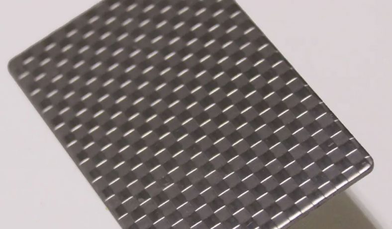
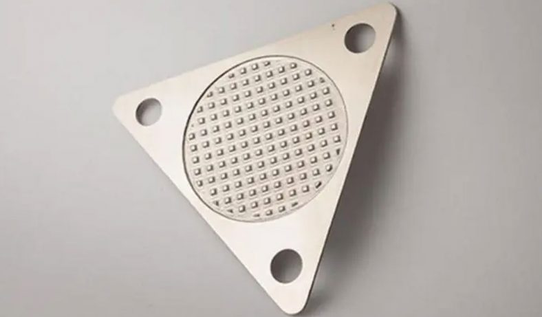
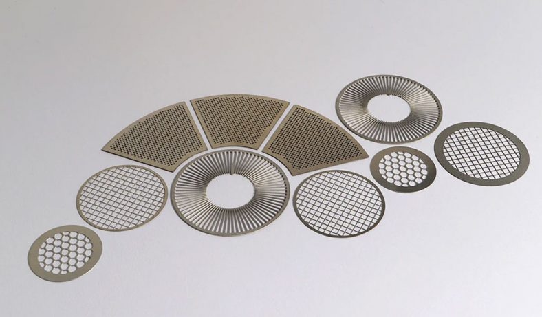
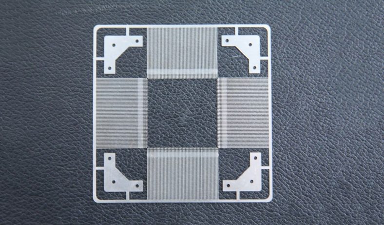
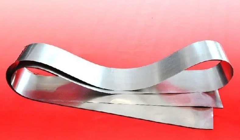
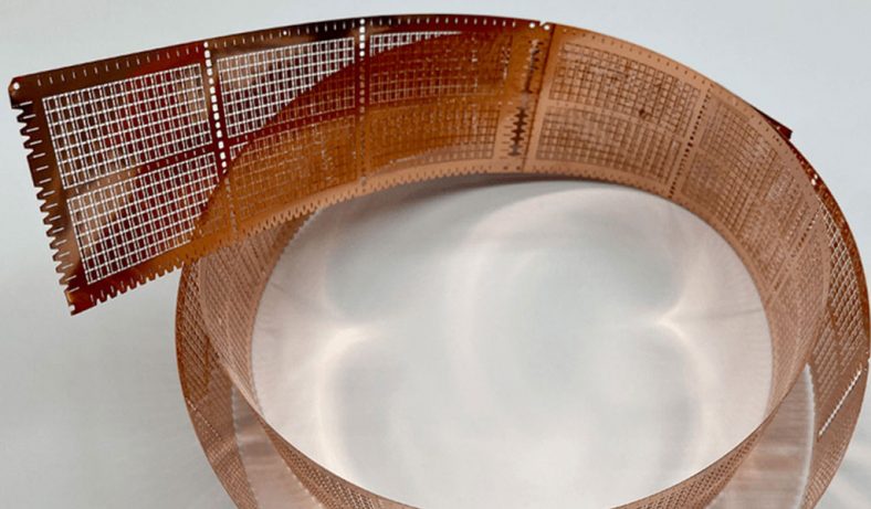
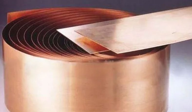
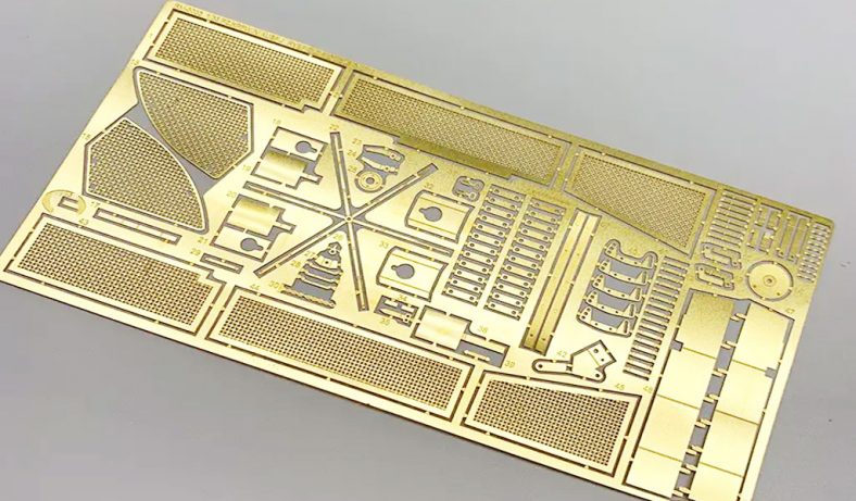
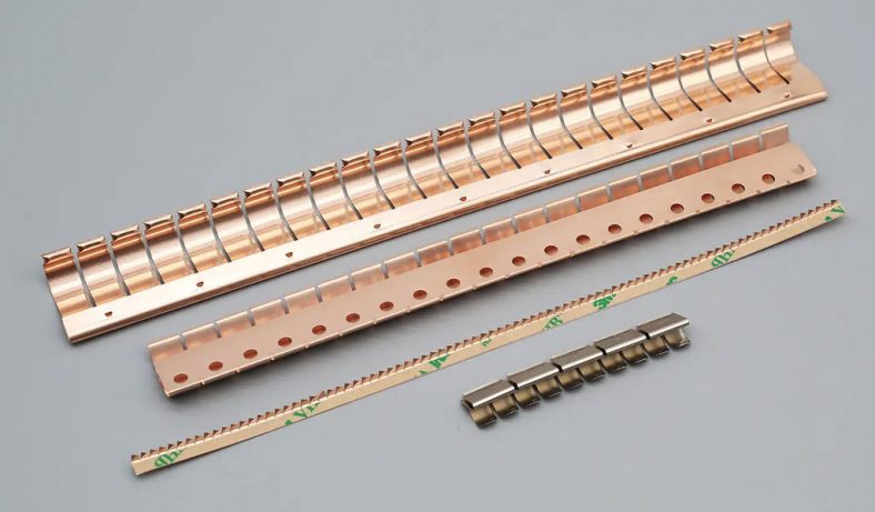
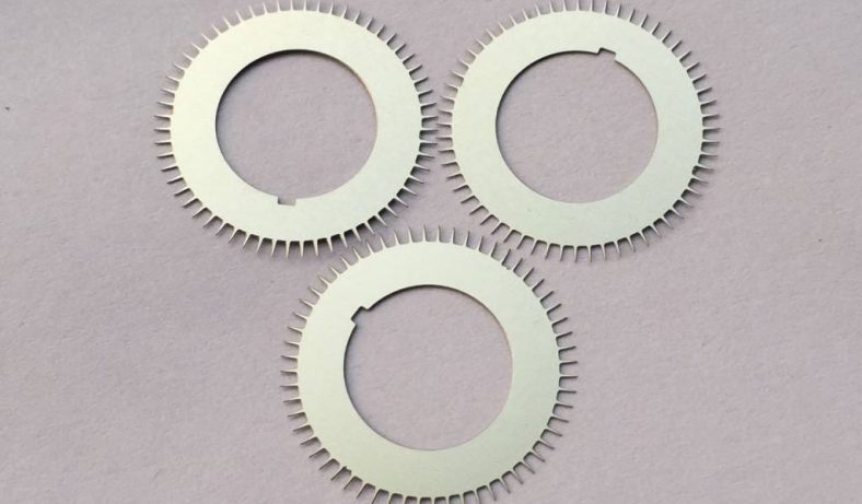
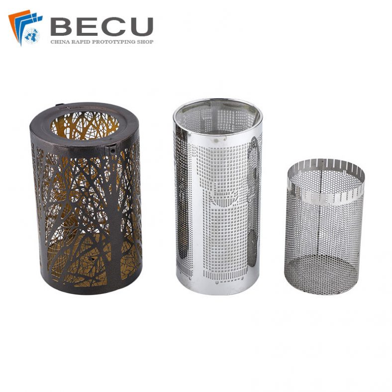
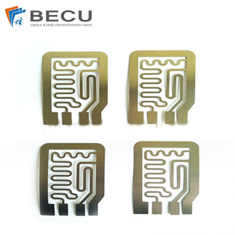
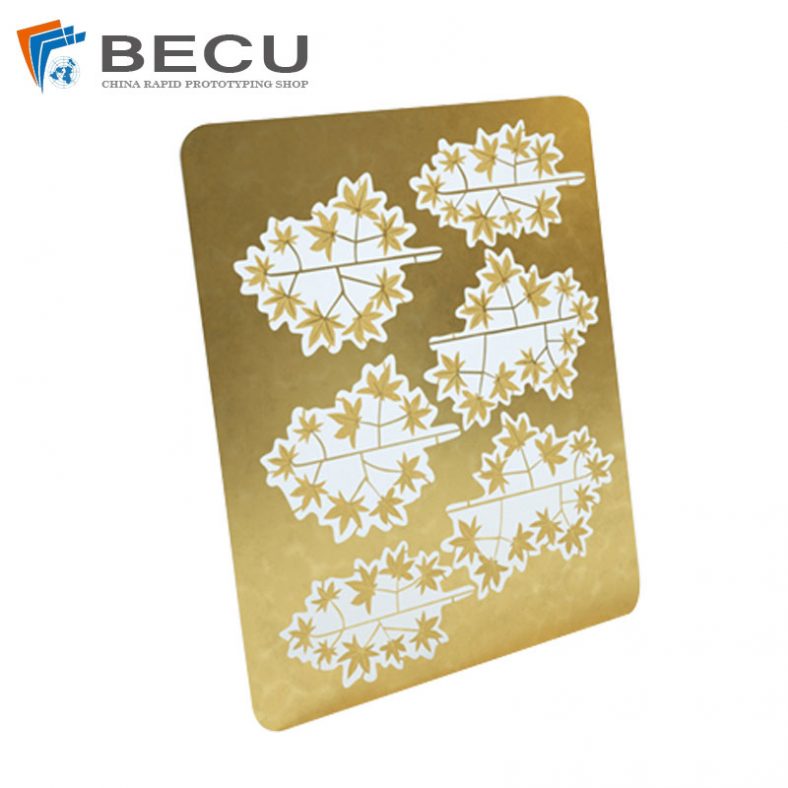
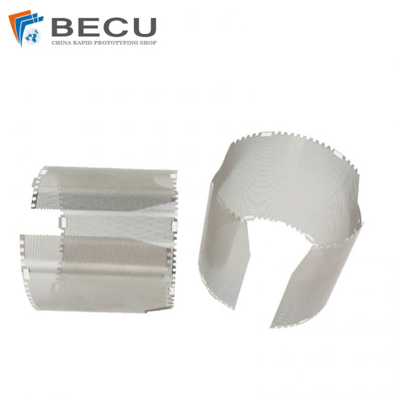
Chemical etching, a subtractive manufacturing process, involves the controlled dissolution of material from a workpiece using chemical reagents, commonly referred to as etchants. This technique has been employed for centuries, with historical applications dating back to ancient Egypt around 2500 BCE, where copper was etched with citric acid for jewelry production. In modern engineering, chemical etching has evolved into a cornerstone of microfabrication, particularly for producing intricate components in microelectronics, microelectromechanical systems (MEMS), and other precision-engineered devices. Copper, prized for its excellent electrical and thermal conductivity, corrosion resistance, and ductility, is a material of choice for microdevices such as printed circuit boards (PCBs), RF/microwave components, and bioelectrical impedance electrodes. The preparation of copper-based microdevices demands high precision, minimal structural compromise, and cost-effective scalability, which traditional etching methods often struggle to achieve consistently.
Recent advancements in chemical etching have introduced innovative approaches to enhance the fabrication of copper-based microdevices. Among these, a novel method combining advanced etchant formulations, optimized process parameters, and surface microstructure engineering has emerged as a promising technique. This method, referred to herein as Enhanced Microstructure Chemical Etching (EMCE), leverages a hybrid etchant system, precise control of etching conditions, and post-etch surface modification to produce copper microdevices with superior dimensional accuracy, surface quality, and functional performance. This article provides a comprehensive exploration of EMCE, detailing its mechanisms, advantages, applications, and comparisons with conventional etching techniques. By addressing the limitations of traditional methods and introducing new possibilities for microdevice fabrication, EMCE represents a significant step forward in materials engineering.
Historical Context of Chemical Etching
Chemical etching, also known as chemical machining, chemical milling, or wet etching, is one of the oldest nontraditional machining processes. Its origins trace back to ancient metallurgical practices, where acidic solutions were used to shape metals decoratively. By the 15th century, chemical etching had replaced hand-tool engraving for producing detailed designs on armor and weaponry, utilizing mineral acids to achieve finer patterns. The industrial application of chemical etching gained momentum in the 20th century, with significant developments post-World War II. In 1956, North American Aviation, Inc. patented the process of “chemical milling” (US Patent No. 2,739,047) for etching aluminum components in aerospace applications, marking a pivotal moment in its adoption for precision manufacturing.
Copper etching, in particular, has been integral to the electronics industry since the advent of PCBs in the mid-20th century. Early etching processes relied on ferric chloride (FeCl₃) as a universal etchant due to its effectiveness across various metals, including copper, steel, and aluminum. However, ferric chloride’s limitations, such as its inability to be economically regenerated for large-scale applications, prompted the exploration of alternative etchants like cupric chloride (CuCl₂) and ammoniacal alkaline solutions. These developments laid the groundwork for modern etching techniques, which prioritize precision, environmental sustainability, and compatibility with advanced microfabrication requirements.
Fundamentals of Chemical Etching
Principles of Etching
Chemical etching operates on the principle of controlled corrosion, where a chemical reagent selectively dissolves material from a workpiece surface. The process typically involves immersing the workpiece in an etchant solution or spraying the etchant onto the surface, with the reaction kinetics governed by factors such as etchant composition, temperature, agitation, and exposure time. For copper, the etching process is a redox reaction, where the etchant oxidizes the copper surface, forming soluble copper ions that are removed from the material.
The general reaction for copper etching with ferric chloride can be expressed as:
[ \text{Cu} + 2\text{FeCl}_3 \rightarrow \text{CuCl}_2 + 2\text{FeCl}_2 ]
In this reaction, ferric ions (Fe³⁺) oxidize copper (Cu) to cupric ions (Cu²⁺), while being reduced to ferrous ions (Fe²⁺). Similarly, cupric chloride etching involves:
[ \text{Cu} + \text{CuCl}_2 \rightarrow 2\text{CuCl} ]
The choice of etchant significantly influences the etch rate, surface roughness, and environmental impact of the process. Etching is often preceded by photolithography, where a photosensitive resist is applied to the copper surface, patterned with UV light, and developed to expose areas for etching, ensuring precise feature definition.
Key Parameters in Chemical Etching
The efficacy of chemical etching depends on several parameters:
- Etchant Composition: The type and concentration of the etchant determine the etch rate and selectivity. Common etchants for copper include FeCl₃, CuCl₂, and hydrogen peroxide-based solutions.
- Temperature: Higher temperatures generally increase etch rates but may compromise surface quality or process control.
- Agitation: Proper agitation ensures uniform etchant distribution, preventing uneven etching or byproduct accumulation.
- Etching Time: The duration of exposure affects the depth of etch and feature resolution.
- Surface Preparation: Pre-etch cleaning and resist application are critical for achieving consistent results.
- Post-Etch Treatment: Surface finishing, such as plating or passivation, enhances the functionality of etched components.
These parameters must be optimized to balance etch rate, precision, and material integrity, particularly for microdevices with features on the order of micrometers.
The Enhanced Microstructure Chemical Etching (EMCE) Method
Overview of EMCE
The Enhanced Microstructure Chemical Etching (EMCE) method is a novel approach designed to address the limitations of conventional copper etching techniques. EMCE integrates a hybrid etchant system, precise process control, and in-situ surface microstructure engineering to produce copper-based microdevices with enhanced performance characteristics. The method is particularly suited for applications requiring high-aspect-ratio features, complex geometries, and stable surface properties, such as bioelectrical impedance electrodes, RF antennas, and microfluidic channels.
EMCE is distinguished by three key innovations:
- Hybrid Etchant System: EMCE employs a synergistic combination of ferric chloride, cupric chloride, and a proprietary organic modifier to achieve high etch rates while maintaining surface smoothness.
- Dynamic Process Control: Advanced monitoring and feedback systems adjust etching parameters in real-time, ensuring uniformity and repeatability across large-scale production.
- In-Situ Microstructure Engineering: During etching, controlled nucleation of microscale surface features enhances the functional properties of the device, such as electrical conductivity or hydrophobicity.
Etchant Formulation
The EMCE etchant is a carefully formulated solution comprising:
- Ferric Chloride (FeCl₃): Provides rapid etch rates due to its strong oxidizing properties. Concentration typically ranges from 300–400 g/L.
- Cupric Chloride (CuCl₂): Enhances surface quality by reducing pitting and roughness. Concentration is maintained at 100–150 g/L.
- Organic Modifier: A benzothiazole-based compound acts as an etch refiner, improving adhesion of subsequent coatings and reducing lateral etching. This modifier is added at 0.5–1.0% by weight.
- Hydrochloric Acid (HCl): Adjusts solution pH and prevents precipitation of iron hydroxides, typically at 1–2% by volume.
- Water: Serves as the solvent, with deionized water used to minimize impurities.
The hybrid etchant is prepared by dissolving FeCl₃ and CuCl₂ in water, followed by the addition of HCl and the organic modifier under controlled conditions. The solution is maintained at a specific gravity of 1.3–1.4 g/cm³ and an oxidation-reduction potential (ORP) of 600–700 mV to ensure consistent etching performance.
Process Workflow
The EMCE process follows a structured workflow:
- Surface Preparation: Copper substrates are cleaned with acetone and isopropyl alcohol to remove contaminants, followed by the application of a photoresist layer.
- Photolithography: The photoresist is exposed to UV light through a mask, defining the desired pattern. The exposed resist is developed, exposing copper areas for etching.
- Etching: The substrate is immersed in the EMCE etchant at 40–50°C, with continuous agitation via a conveyorized spray system. Etching time ranges from 5–20 minutes, depending on feature depth.
- In-Situ Microstructure Formation: During etching, the organic modifier induces controlled nucleation of microscale features, such as nanorods or micropores, on the copper surface.
- Post-Etch Treatment: The substrate is rinsed with deionized water, stripped of resist, and optionally plated with nickel or silver to enhance corrosion resistance.
- Characterization: Etched components undergo dimensional inspection, surface roughness analysis, and functional testing to verify compliance with specifications.
Mechanisms of EMCE
The EMCE process leverages a combination of electrochemical and chemical mechanisms to achieve its results. The ferric chloride component drives rapid oxidation of the copper surface, forming soluble CuCl₂. The cupric chloride, acting as a secondary oxidant, refines the etch profile by minimizing undercutting and promoting anisotropic etching. The organic modifier plays a dual role:
- Surface Passivation: It adsorbs onto the copper surface, reducing lateral etching and enhancing feature resolution.
- Microstructure Nucleation: It facilitates the formation of ordered microstructures by modulating the redox reaction kinetics, leading to controlled surface roughening.
The dynamic process control system monitors key parameters such as etchant temperature, ORP, and copper ion concentration, adjusting them in real-time to maintain optimal conditions. This ensures uniformity across large substrates and minimizes defects such as over-etching or pitting.
Advantages of EMCE
EMCE offers several advantages over conventional etching methods, making it a transformative approach for copper-based microdevice fabrication:
- High Precision: EMCE achieves dimensional tolerances of ±0.020 mm, enabling the production of intricate features with high aspect ratios.
- Superior Surface Quality: The hybrid etchant reduces surface roughness (Ra) to below 0.5 µm, compared to 1–2 µm for FeCl₃-based etching.
- Scalability: The process is compatible with high-throughput manufacturing, with low-cost tooling and rapid prototyping capabilities.
- Environmental Sustainability: The organic modifier reduces etchant consumption, and the system allows for partial regeneration of CuCl₂, minimizing waste.
- Functional Enhancement: In-situ microstructure engineering improves device performance, such as increasing contact stability in bioelectrical electrodes or enhancing hydrophobicity in microfluidic devices.
Comparison with Conventional Etching Methods
To illustrate the advantages of EMCE, Table 1 compares its performance with three conventional etching methods: ferric chloride etching, cupric chloride etching, and metal-assisted chemical etching (MACE).
| Parameter | EMCE | Ferric Chloride Etching | Cupric Chloride Etching | MACE |
|---|---|---|---|---|
| Etchant Composition | FeCl₃, CuCl₂, Organic Modifier, HCl | FeCl₃, HCl | CuCl₂, HCl | HF, H₂O₂, Metal Catalyst (e.g., Cu) |
| Etch Rate (µm/min) | 1.0–2.0 | 2.0–3.0 | 0.5–1.0 | 0.1–0.5 |
| Surface Roughness (Ra, µm) | 0.3–0.5 | 1.0–2.0 | 0.5–0.8 | 0.8–1.5 |
| Dimensional Tolerance (mm) | ±0.020 | ±0.050 | ±0.030 | ±0.100 |
| Feature Resolution (µm) | 10 | 50 | 20 | 100 |
| Environmental Impact | Moderate (partial regeneration) | High (non-regenerable) | Moderate (regenerable) | High (HF toxicity) |
| Cost of Tooling | Low | Low | Low | High |
| Scalability | High | Moderate | High | Low |
| Microstructure Control | High (in-situ engineering) | Low | Moderate | High (nanoscale focus) |
| Applications | PCBs, Bioelectrodes, RF Components | PCBs, Decorative Etching | PCBs, Precision Parts | Nanostructures, MEMS |
Table 1: Comparison of EMCE with conventional copper etching methods. Data compiled from references,,, and industry standards.
Analysis of Table 1
- Etch Rate: EMCE offers a balanced etch rate, faster than CuCl₂ and MACE but slower than FeCl₃, prioritizing precision over speed.
- Surface Roughness: EMCE achieves the lowest Ra, making it ideal for applications requiring smooth surfaces, such as RF components.
- Dimensional Tolerance: EMCE’s tight tolerances (±0.020 mm) surpass all competitors, enabling high-precision microdevices.
- Environmental Impact: While not fully regenerable, EMCE’s partial CuCl₂ regeneration reduces waste compared to FeCl₃, and it avoids the toxicity of HF used in MACE.
- Microstructure Control: EMCE’s in-situ engineering provides unique control over surface features, unlike FeCl₃ and CuCl₂, which offer limited microstructure modulation.
Applications of EMCE in Copper-Based Microdevices
Printed Circuit Boards (PCBs)
PCBs are the backbone of modern electronics, relying on copper for conductive traces. EMCE enhances PCB fabrication by producing fine-line patterns with linewidths as small as 10 µm, compared to 50 µm for FeCl₃ etching. The method’s high precision and smooth surfaces reduce signal loss in high-frequency applications, such as 5G communication systems. Additionally, the organic modifier improves adhesion of solder masks and imaging resists, addressing challenges in lead-free PCB production.
Bioelectrical Impedance Electrodes
Bioelectrical impedance electrodes, used in medical diagnostics, require stable contact with biological tissues. EMCE’s ability to engineer microscale surface features, such as micropores, enhances electrode stability, as demonstrated by impedance tests showing 24-hour stability superior to commercial ECG electrodes. The method’s compatibility with biocompatible coatings, such as silver plating, further expands its medical applications.
RF and Microwave Components
RF and microwave components, such as antennas and waveguides, demand high electrical conductivity and minimal surface roughness to minimize signal attenuation. EMCE’s smooth etch profiles and precise feature definition make it ideal for fabricating compact, high-performance RF devices. For example, EMCE has been used to produce microstrip antennas with improved gain and bandwidth compared to laser-cut alternatives.
Microfluidic Devices
Microfluidic devices, used in chemical and biological analysis, benefit from EMCE’s ability to create hydrophobic surfaces through microstructure engineering. Superhydrophobic copper meshes, etched with EMCE and coated with stearic acid, have demonstrated oil-water separation efficiencies above 97% after multiple cycles. These devices are critical for environmental applications, such as oil spill remediation.
Challenges and Limitations
Despite its advantages, EMCE faces several challenges:
- Complexity of Etchant Management: The hybrid etchant requires precise formulation and monitoring, increasing operational complexity compared to single-etchant systems.
- Cost of Organic Modifier: The proprietary benzothiazole compound adds to material costs, though this is offset by reduced etchant consumption.
- Limited Regeneration: While CuCl₂ can be partially regenerated, FeCl₃ remains non-regenerable, posing environmental challenges for large-scale applications.
- Process Sensitivity: EMCE’s reliance on dynamic process control demands advanced equipment, which may be a barrier for small-scale manufacturers.
Future research aims to address these limitations by developing fully regenerable etchants, reducing the cost of organic modifiers, and simplifying process control systems.
Future Directions
The development of EMCE opens several avenues for future innovation:
- Integration with Additive Manufacturing: Combining EMCE with 3D printing could enable hybrid fabrication of complex copper structures, blending subtractive and additive techniques.
- Sustainable Etchant Formulations: Research into biodegradable or fully regenerable etchants could enhance EMCE’s environmental profile.
- AI-Driven Process Optimization: Machine learning algorithms could further refine dynamic process control, predicting optimal etching conditions for diverse substrates.
- Expansion to Other Materials: Adapting EMCE for other conductive metals, such as silver or gold, could broaden its application in advanced electronics.
Conclusion
Enhanced Microstructure Chemical Etching (EMCE) represents a paradigm shift in the fabrication of copper-based microdevices. By integrating a hybrid etchant system, dynamic process control, and in-situ microstructure engineering, EMCE achieves unparalleled precision, surface quality, and functional performance. Its applications span PCBs, bioelectrical electrodes, RF components, and microfluidic devices, addressing critical needs in electronics, medical diagnostics, and environmental engineering. While challenges such as etchant management and cost remain, ongoing research promises to overcome these hurdles, positioning EMCE as a cornerstone of next-generation microfabrication. As the demand for smaller, more efficient microdevices grows, EMCE’s ability to deliver high-performance solutions underscores its transformative potential in materials science and engineering.

