
Microfluidic chips, often referred to as “lab-on-a-chip” devices, have revolutionized fields such as biomedical diagnostics, chemical analysis, and materials science by enabling precise manipulation of fluids at the microscale. These devices typically consist of microchannels, chambers, and other microstructures etched or molded into substrates like glass, silicon, or polymers such as polydimethylsiloxane (PDMS). Among the various materials used, gold has emerged as a particularly valuable component in microfluidic systems due to its unique properties, including high electrical conductivity, chemical inertness, biocompatibility, and plasmonic behavior. Gold-based microfluidic chips are employed in applications ranging from biosensors and polymerase chain reaction (PCR) systems to plasmonic sensing and electrochemical detection.
The fabrication of gold-based microfluidic chips requires precise patterning and structuring of gold thin films or nanostructures, often integrated with other substrate materials. Plasma etching, a dry etching technique widely used in semiconductor manufacturing, has become a critical process for achieving the high-resolution, anisotropic patterns necessary for these devices. Unlike wet etching, which can lead to isotropic etching and undercutting, plasma etching offers superior control over feature sizes, sidewall profiles, and surface quality, making it ideal for micro- and nanofabrication. This article provides a comprehensive exploration of the application of plasma etching in the fabrication of gold-based microfluidic chips, covering its principles, techniques, challenges, and specific applications. It also examines the integration of gold with microfluidic substrates, recent advancements, and future prospects, supported by detailed comparative tables.
Principles of Plasma Etching
Overview of Plasma Etching
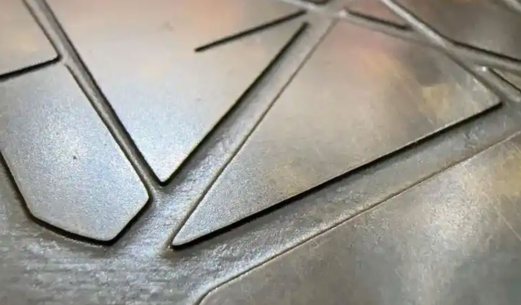
Plasma etching is a dry etching process that utilizes a partially ionized gas (plasma) to remove material from a substrate surface. The plasma, often generated by applying radio-frequency (RF) power to a gas mixture, contains reactive species such as ions, radicals, and electrons. These species interact with the substrate to form volatile etch products, which are subsequently removed by a vacuum system. Plasma etching is distinguished from wet etching by its ability to produce anisotropic (directional) etch profiles, making it suitable for high-aspect-ratio structures and submicron features.
The process occurs in a vacuum chamber where a substrate, typically coated with a patterned mask (e.g., photoresist or metal), is exposed to the plasma. The mask protects certain areas of the substrate, allowing selective etching of exposed regions. Common plasma sources include capacitively coupled plasma (CCP), inductively coupled plasma (ICP), and electron cyclotron resonance (ECR) plasma, each offering different levels of plasma density and ion energy.
Mechanisms of Plasma Etching
Plasma etching involves both physical and chemical mechanisms. The physical component arises from ion bombardment, where energetic ions strike the substrate surface, breaking chemical bonds and ejecting material. This process, often referred to as sputtering, enhances anisotropy by preferentially etching in the direction of ion incidence (typically perpendicular to the substrate). The chemical component involves reactions between reactive radicals or ions and the substrate material, forming volatile products that desorb from the surface. For example, in the etching of silicon, fluorine-based plasmas (e.g., SF6) react to form volatile SiF4.
In the context of gold etching, the chemical mechanism is complicated by gold’s low reactivity and the limited volatility of gold etch products. Gold does not readily form volatile compounds with common etchants like fluorine or oxygen, necessitating specialized chemistries, such as chlorine-based plasmas, which form volatile gold chlorides (e.g., AuCl3). The interplay between physical sputtering and chemical etching is critical to achieving high etch rates and clean profiles.
Types of Plasma Etching for Gold
Several plasma etching techniques are employed for gold patterning in microfluidic chips, including:
- Reactive Ion Etching (RIE): RIE combines chemical etching with ion bombardment, using a plasma generated by an RF source. The substrate is placed on a biased electrode, attracting ions that enhance anisotropy. RIE is widely used for gold etching due to its balance of etch rate and profile control.
- Inductively Coupled Plasma Reactive Ion Etching (ICP-RIE): ICP-RIE uses a high-density plasma generated by an inductively coupled RF source, offering higher etch rates and better uniformity than traditional RIE. It is particularly effective for deep etching and high-aspect-ratio structures.
- Deep Reactive Ion Etching (DRIE): DRIE, often associated with the Bosch process for silicon, has been adapted for gold etching in specialized applications. It involves alternating cycles of etching and passivation to achieve deep, vertical features.
- Plasma-Enhanced Etching: This variant uses plasma to enhance chemical reactions without significant ion bombardment, suitable for delicate substrates or isotropic etching.
Each technique has specific advantages and limitations, which are discussed in subsequent sections and summarized in comparative tables.
Gold in Microfluidic Chips
Properties of Gold Relevant to Microfluidics
Gold’s unique properties make it an ideal material for microfluidic applications:
- Electrical Conductivity: Gold’s high conductivity (resistivity ~2.44 × 10⁻⁸ Ω·m) enables its use in electrodes for electrochemical sensing and actuation.
- Chemical Inertness: Gold resists corrosion and oxidation, ensuring stability in harsh chemical environments, such as those encountered in biological assays.
- Biocompatibility: Gold is non-toxic and compatible with biological samples, making it suitable for biomedical applications like cell culture and DNA analysis.
- Plasmonic Properties: Gold exhibits surface plasmon resonance (SPR), enabling optical sensing and photothermal effects in microfluidic systems.
- Surface Functionalization: Gold surfaces can be easily modified with thiol-based self-assembled monolayers (SAMs), facilitating biomolecule attachment for biosensors.
These properties underpin gold’s role in microfluidic chips, where it is used as thin films, nanoparticles, or nanostructured surfaces.
Applications of Gold in Microfluidic Chips
Gold-based microfluidic chips are employed in diverse applications, including:
- Biosensors: Gold electrodes or nanoparticles enhance sensitivity in electrochemical or SPR-based biosensors for detecting proteins, DNA, or pathogens.
- PCR Systems: Gold nanofilms enable rapid photothermal cycling in droplet-based photonic PCR, as demonstrated in a 2021 study where a gold nanofilm-based chip achieved 30 thermal cycles in 13 minutes.
- Electrochemical Detection: Gold electrodes facilitate precise measurement of redox reactions in lab-on-a-chip devices.
- Plasmonic Sensing: Gold nanostructures support localized surface plasmon resonance (LSPR) for label-free detection of analytes.
- Microfluidic Valves and Pumps: Gold’s conductivity enables electrokinetic actuation in microfluidic systems.
These applications require precise patterning of gold, often at submicron scales, which plasma etching is well-suited to achieve.
Plasma Etching of Gold for Microfluidic Chip Fabrication
Challenges in Gold Etching
Etching gold poses several challenges due to its chemical and physical properties:
- Low Volatility of Etch Products: Gold chlorides (e.g., AuCl3) have relatively high boiling points (~265°C for AuCl3), requiring high ion energy or elevated substrate temperatures to desorb etch products. This contrasts with silicon etching, where SiF4 is volatile at room temperature.
- Mask Selectivity: Gold etching often requires robust masks (e.g., nickel or chromium) to withstand aggressive plasma conditions, as photoresists may erode quickly.
- Surface Roughness: Ion bombardment can increase surface roughness, affecting optical or electrical properties in microfluidic applications.
- Residue Formation: Non-volatile etch byproducts can redeposit on the substrate, necessitating post-etch cleaning.
- Anisotropy Control: Achieving vertical sidewalls is critical for high-aspect-ratio features but can be difficult due to gold’s resistance to chemical etching.
These challenges have driven the development of specialized plasma etching processes for gold, particularly chlorine-based chemistries and high-density plasma systems.
Chlorine-Based Plasma Etching
Chlorine-based plasmas, typically using Cl2 or Cl2/Ar mixtures, are the most common for gold etching. The process involves:
- Chemical Reaction: Chlorine radicals react with gold to form AuClx compounds. The reaction is enhanced by ion bombardment, which breaks gold-gold bonds and promotes chloride formation.
- Physical Sputtering: Argon ions in Cl2/Ar plasmas sputter non-volatile AuClx, aiding removal and preventing redeposition.
- Process Optimization: Parameters such as gas ratio, RF power, bias voltage, and chamber pressure are tuned to balance etch rate, anisotropy, and surface quality.
A 2024 study demonstrated gold etching with a Cl2/(Cl2+Ar) ratio of 0.2, achieving an etch rate of 3500 Å/min and a selectivity of 4.4 to SiO2 at 700 W RF power and -150 V bias. X-ray photoelectron spectroscopy (XPS) confirmed the formation of Au-Cl bonds, with Ar ion bombardment removing high-melting-point residues.
Table 1: Comparison of Chlorine-Based Plasma Etching Parameters for Gold
| Parameter | Typical Range | Effect on Etching Process | Reference |
|---|---|---|---|
| Cl2/(Cl2+Ar) Ratio | 0.1–0.5 | Higher Cl2 increases chemical etching; Ar enhances sputtering | |
| RF Power | 500–1000 W | Increases plasma density and etch rate | |
| Bias Voltage | -100 to -200 V | Enhances ion bombardment, improving anisotropy | |
| Chamber Pressure | 10–20 mTorr | Lower pressure improves anisotropy; higher pressure increases etch rate | |
| Substrate Temperature | 20–100°C | Higher temperatures aid desorption of AuClx | |
| Etch Rate | 1000–3500 Å/min | Depends on gas chemistry and power | |
| Selectivity (Au:SiO2) | 2–4.4 | Higher selectivity with optimized Cl2/Ar ratio |
Hydrogen-Based Plasma Etching
Emerging research has explored hydrogen-based plasmas (e.g., H2 or H2/Ar) for gold etching, particularly for applications requiring minimal surface damage. Hydrogen plasmas produce volatile gold hydrides, which desorb more readily than chlorides. However, hydrogen etching is less common due to lower etch rates and challenges in maintaining anisotropy. A 2014 review noted that hydrogen plasmas show promise for gold nanofabrication but require further optimization.
Mask Materials and Selectivity
The choice of mask material is critical in gold etching. Common masks include:
- Nickel (Ni): Electroplated Ni masks offer high selectivity and durability, as demonstrated in glass etching studies where Ni withstood fluorine plasmas.
- Chromium (Cr): Cr masks are used in ICP-RIE of SiC and can be adapted for gold, with selectivity influenced by O2 addition to SF6 plasmas.
- Photoresist: Photoresists are less robust but suitable for shallow etching or low-power plasmas. Oxygen plasma treatment can enhance photoresist adhesion to substrates like PDMS.
Selectivity (the ratio of gold etch rate to mask etch rate) is a key metric. For example, a Cr mask in Cl2/Ar plasma achieved a selectivity of 4.4 to SiO2, sufficient for microfluidic channel patterning.
Table 2: Mask Materials for Gold Plasma Etching
| Mask Material | Selectivity (Au:Mask) | Advantages | Disadvantages | Reference |
|---|---|---|---|---|
| Nickel (Ni) | 5–10 | High durability, reusable | Requires electroplating, costly | |
| Chromium (Cr) | 3–5 | Good selectivity, easy deposition | Limited durability in aggressive plasmas | |
| Photoresist | 1–3 | Easy to pattern, cost-effective | Low durability, prone to erosion | |
| SiO2 | 2–4.4 | Compatible with semiconductor processes | Requires additional deposition steps |
Integration with Microfluidic Substrates
Gold-based microfluidic chips often combine gold with substrates like glass, silicon, or PDMS. Plasma etching must be tailored to ensure compatibility:
- Glass Substrates: Glass microfluidic chips, etched using fluorine plasmas (e.g., C4F8/O2), can incorporate gold electrodes. A 2010 study achieved 100 μm deep glass channels with an 83°–88° profile angle using ICP-RIE, followed by gold deposition and patterning.
- Silicon Substrates: Silicon is etched with SF6-based DRIE, and gold is patterned using Cl2/Ar plasmas. Silicon’s compatibility with semiconductor processes makes it ideal for integrated devices.
- PDMS Substrates: PDMS is etched with SF6/O2 plasmas, and gold nanofilms are bonded using adhesive techniques. A 2021 study used a gold nanofilm on PDMS for photonic PCR, with plasma etching defining microfluidic channels.
Integration requires careful process sequencing to avoid damage to gold or substrate materials. For example, gold etching is typically performed after substrate channel etching to prevent exposure to fluorine plasmas, which can erode gold.
Fabrication Processes for Gold-Based Microfluidic Chips
Process Flow
A typical fabrication process for a gold-based microfluidic chip involves:
- Substrate Preparation: Cleaning the substrate (e.g., glass, silicon, or PDMS) to remove contaminants.
- Channel Etching: Etching microchannels using plasma etching (e.g., SF6/O2 for PDMS, C4F8/O2 for glass).
- Gold Deposition: Depositing a gold thin film via sputtering, evaporation, or chemical vapor deposition (CVD).
- Mask Patterning: Applying a mask (e.g., photoresist or Ni) using photolithography.
- Gold Etching: Patterning the gold film using Cl2/Ar plasma etching.
- Mask Removal: Stripping the mask using wet or plasma-based methods.
- Bonding: Sealing the microfluidic chip with a cover layer (e.g., glass or PDMS) using anodic bonding, adhesive bonding, or plasma bonding.
- Surface Functionalization: Modifying gold surfaces with thiols or other molecules for specific applications.
Case Study: Gold Nanofilm-Based Photonic PCR Chip
A 2021 study demonstrated a gold nanofilm-based microfluidic chip for droplet-based photonic PCR. The fabrication process involved:
- PDMS Channel Etching: SF6/O2 ICP-RIE etched 600 μm deep channels in PDMS, with a 10 mTorr pressure and 500 W RF power.
- Gold Deposition: A 50 nm gold nanofilm was sputtered onto the PDMS substrate.
- Gold Patterning: Cl2/Ar plasma etching defined gold electrodes, achieving a 2000 Å/min etch rate with a Ni mask.
- Bonding: The PDMS slab was bonded to the gold nanofilm using double-sided adhesive tape, suppressing droplet evaporation during PCR thermocycling.
- Testing: The chip performed 30 thermal cycles in 13 minutes, with heating rates of 7.37°C/s, enabled by the gold nanofilm’s photothermal properties.
This case highlights the synergy between plasma etching and gold’s plasmonic properties, enabling rapid, high-performance microfluidic devices.
Table 3: Fabrication Steps for Gold-Based Microfluidic Chips
| Step | Technique | Parameters | Substrate Compatibility | Reference |
|---|---|---|---|---|
| Channel Etching | ICP-RIE (SF6/O2, C4F8/O2) | 10–30 mTorr, 500–1000 W | Glass, Silicon, PDMS | , |
| Gold Deposition | Sputtering, Evaporation | 10–50 nm thickness | All substrates | |
| Mask Patterning | Photolithography | Photoresist or Ni mask | All substrates | |
| Gold Etching | Cl2/Ar ICP-RIE | 0.1–0.5 Cl2 ratio, 500–700 W | Gold films | |
| Mask Removal | Wet Etching, O2 Plasma | Acetone or O2 plasma for photoresist | All substrates | |
| Bonding | Anodic, Adhesive, Plasma | 350°C for glass, adhesive for PDMS | Glass, PDMS | , |
| Functionalization | Thiol SAMs | 1–10 mM thiol concentration | Gold surfaces |
Scalability and Cost Considerations
Plasma etching enables scalable fabrication of gold-based microfluidic chips, as it is compatible with semiconductor manufacturing infrastructure. However, costs are influenced by:
- Equipment: ICP-RIE systems are expensive, with capital costs exceeding $500,000.
- Materials: Gold and Ni masks are costly compared to photoresists.
- Throughput: High-density plasma systems like ICP-RIE offer faster etch rates, improving throughput but requiring skilled operators.
Low-cost alternatives, such as laser machining for PDMS chips, have been explored, but plasma etching remains superior for submicron precision.
Applications in Biomedical and Analytical Systems
Biosensors and Diagnostics
Gold-based microfluidic chips are widely used in biosensors for point-of-care diagnostics. Plasma-etched gold electrodes enable:
- Electrochemical Sensing: Gold’s conductivity supports amperometric or voltammetric detection of biomarkers like glucose or cardiac troponins.
- SPR-Based Detection: Gold nanostructures, patterned via plasma etching, enhance SPR sensitivity for label-free detection of DNA or proteins.
A 2016 study integrated gold electrodes in a PDMS microfluidic chip for electrochemical detection of cancer biomarkers, using Cl2/Ar plasma to pattern 100 nm thick gold films.
Photonic PCR and DNA Amplification
Gold nanofilms in microfluidic chips enable rapid PCR through plasmonic photothermal heating. The 2021 photonic PCR chip used a gold nanofilm to achieve heating rates of 7.37°C/s, significantly faster than conventional PCR systems. Plasma etching defined the nanofilm’s geometry, ensuring uniform heating across droplets.
Lab-on-a-Chip Systems
Gold-based microfluidic chips integrate multiple functions (e.g., mixing, separation, detection) on a single platform. Plasma etching creates high-aspect-ratio channels and gold electrodes, enabling compact, multifunctional devices. For example, a 2018 study used ICP-RIE to fabricate a silicon-based chip with gold electrodes for peptide analysis, achieving sub-nanoliter sample manipulation.
Table 4: Applications of Gold-Based Microfluidic Chips
| Application | Gold Component | Plasma Etching Role | Performance Metrics | Reference |
|---|---|---|---|---|
| Biosensors | Electrodes, Nanoparticles | Patterning electrodes, nanostructures | Sensitivity: 1 pM–1 nM | |
| Photonic PCR | Nanofilms | Defining photothermal layers | 30 cycles in 13 min, 7.37°C/s heating | |
| Electrochemical Detection | Electrodes | High-resolution electrode patterning | Detection limit: 0.1–10 μM | |
| Plasmonic Sensing | Nanostructures | Fabricating LSPR structures | Sensitivity: 500 nm/RIU | |
| Lab-on-a-Chip | Electrodes, Actuators | Creating multifunctional structures | Sample volume: 0.1–1 nL |
Advances and Innovations
High-Density Plasma Systems
Recent advancements in high-density plasma systems, such as ICP-RIE and ECR plasma, have improved gold etching for microfluidic applications. These systems offer:
- Higher Etch Rates: ICP-RIE achieves up to 3500 Å/min for gold, compared to 1000 Å/min for conventional RIE.
- Better Uniformity: High-density plasmas ensure consistent etching across large wafers, critical for scalable production.
- Reduced Surface Damage: Optimized chemistries minimize roughness, preserving gold’s optical and electrical properties.
A 2024 review highlighted the role of high-NA EUV lithography and plasma etching in scaling feature sizes below 100 nm, relevant for next-generation microfluidic chips.
Alternative Chemistries
Beyond chlorine and hydrogen plasmas, alternative chemistries are being explored:
- Sulfuryl Chloride (SO2Cl2): Used in thermal atomic layer etching (ALE) of gold, offering atomic-scale precision for nanostructures.
- Fluorine-Based Plasmas: While less common for gold, fluorine plasmas (e.g., CF4) are used in hybrid chips to etch substrates like glass or silicon before gold deposition.
Environmental Considerations
Plasma etching’s environmental impact, particularly the use of fluorinated etchants, is a growing concern. Per- and polyfluoroalkyl substances (PFAS) in etchants contribute to greenhouse gas emissions and require abatement systems. A 2024 study emphasized the need for water treatment to manage PFAS waste, relevant for gold etching facilities. Alternative chemistries, such as hydrogen-based plasmas, may reduce environmental impact.
Challenges and Future Directions
Technical Challenges
Despite advancements, challenges persist:
- Etch Product Volatility: Gold chlorides’ high boiling points limit etch rates, requiring high ion energies that may damage substrates.
- Cost: High-density plasma systems and gold materials increase fabrication costs, limiting accessibility for small-scale labs.
- Scalability: While plasma etching is scalable, integrating gold with flexible substrates like PDMS requires further process development.
Future Prospects
Future developments in gold-based microfluidic chips include:
- Atomic Layer Etching (ALE): ALE offers sub-nanometer precision, ideal for nanostructured gold surfaces in plasmonic sensors.
- Hybrid Materials: Combining gold with 2D materials (e.g., graphene) could enhance sensor performance, with plasma etching defining hybrid structures.
- Sustainable Processes: Developing low-impact etchants and recycling systems will address environmental concerns.
- Point-of-Care Diagnostics: Plasma-etched gold chips could enable affordable, portable diagnostic devices for global health applications.
Conclusion
Plasma etching is a cornerstone of gold-based microfluidic chip fabrication, enabling precise patterning of gold thin films and nanostructures for applications in biosensing, PCR, and lab-on-a-chip systems. Chlorine-based ICP-RIE dominates gold etching due to its high etch rates and anisotropy, though challenges like low etch product volatility and environmental impact persist. Advances in high-density plasma systems, alternative chemistries, and integration with substrates like glass and PDMS have expanded the capabilities of gold-based microfluidics. As the field evolves, innovations in atomic layer etching, sustainable processes, and hybrid materials promise to further enhance performance and accessibility. This article provides a comprehensive foundation for researchers and engineers seeking to leverage plasma etching in the development of next-generation microfluidic devices.


