In dry etching, gases are excited by high-frequency sources (primarily 13.56 MHz or 2.45 GHz). At pressures ranging from 1 to 100 Pa, the average free path is several millimeters to centimeters.There are three main types of dry etching:
- Physical Dry Etching: Accelerated particles cause physical abrasion on the wafer surface.
- Chemical Dry Etching: Gases chemically react with the wafer surface.
- Chemical-Physical Dry Etching: A hybrid etching process combining physical and chemical characteristics.
1. Ion Beam Etching
Ion beam etching is a physical dry etching process. In this method, argon ions are accelerated and directed at the surface with an ion beam of about 1 to 3 keV. Due to the ions’ energy, they bombard the surface material. The wafer is positioned either vertically or tilted into the ion beam, resulting in an absolutely anisotropic etching process. The selectivity is low because there is no distinction between different layers. Gases and abraded material are pumped out by a vacuum pump; however, since the reaction products are not gaseous, particles can deposit on the wafer or the chamber walls.
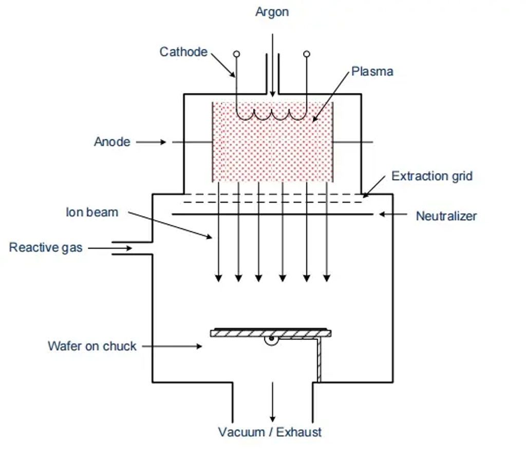
To prevent particle deposition, a second gas is introduced into the chamber. This gas reacts with argon ions, initiating a physical-chemical etching process. Some of the gas reacts with the surface, while others react with the abraded particles to form gaseous byproducts. Almost all materials can be etched using this method. Due to vertical irradiation, the abrasion on vertical walls is very low (high anisotropy). However, due to low selectivity and low etch rate, this process is rarely used in modern semiconductor manufacturing.
2. Plasma Etching
Plasma etching is an entirely chemical etching process (chemical dry etching). The advantage is that the wafer surface is not damaged by accelerated ions. Due to the mobile particles of the etching gas, the etching profile is isotropic, making this method suitable for removing entire film layers (e.g., cleaning the backside after thermal oxidation).
A type of reactor used for plasma etching is the downstream reactor. Here, plasma is ignited at 2.45 GHz via collision ionization, with the ionization occurring away from the wafer.
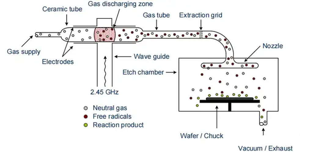
In the gas discharge area, various particles, including radicals, are present due to collisions. Radicals are neutral atoms or molecules with unsatisfied electrons, making them highly reactive. For instance, tetrafluoromethane (CF4) is introduced into the gas discharge area and dissociates into CF2 and fluorine molecules (F2). Similarly, fluorine can be separated from CF4 by adding oxygen (O2):
2 CF4 + O2 —> 2 COF2 + 2 F2
Fluorine molecules can be split into individual fluorine atoms by the energy in the gas discharge area. Each fluorine atom is a fluorine radical, as each atom has seven valence electrons and seeks to achieve an inert gas configuration. Besides neutral radicals, several partially charged particles (CF+4, CF+3, CF+2, …) are also present.
All these particles, radicals, etc., then enter the etching chamber through a ceramic tube. Charged particles can be blocked from the etching chamber by an extraction grid or recombine on their way to becoming neutral molecules. Fluorine radicals also partially recombine but enough reach the etching chamber to react with the wafer surface, causing chemical abrasion. Other neutral particles are not part of the etching process and are depleted along with the reaction products.
Examples of thin films that can be etched in plasma etching include:
- Silicon: Si + 4F —> SiF4
- Silicon Dioxide: SiO2 + 4F —> SiF4 + O2
- Silicon Nitride: Si3N4 + 12F —> 3SiF4 + 2N2
3. Reactive Ion Etching (RIE)
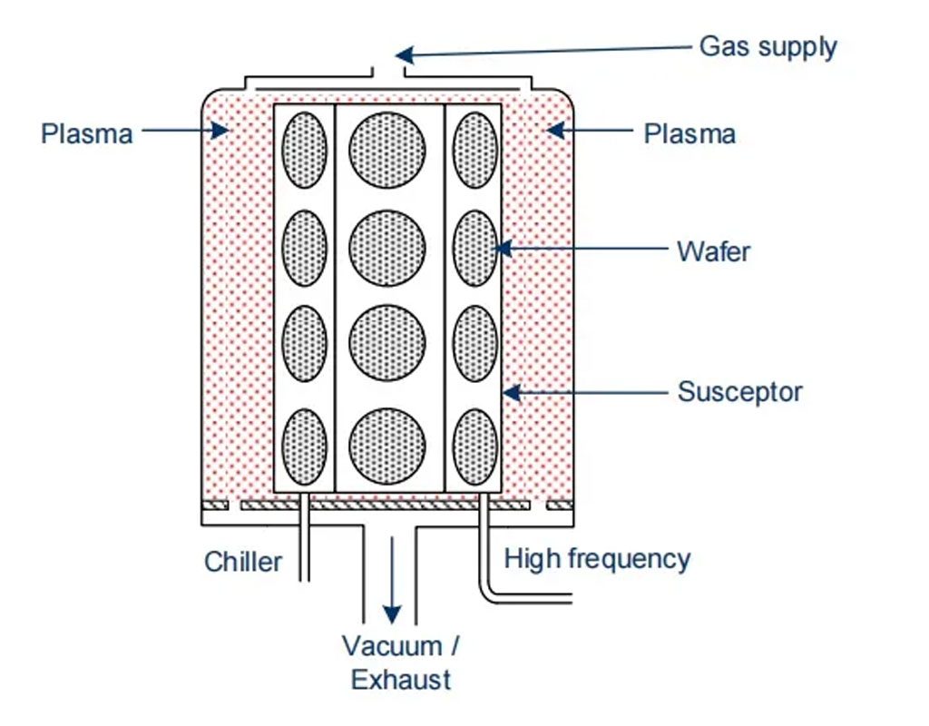
Etching characteristics such as selectivity, etching profile, etch rate, uniformity, and reproducibility can be precisely controlled in reactive ion etching (RIE). Both isotropic and anisotropic etching profiles are possible. Therefore, RIE is a chemical-physical etching process and is one of the most important processes in semiconductor manufacturing for constructing various thin films. In the processing chamber, the wafer is placed on a high-frequency electrode (HF electrode). Plasma is generated through collision ionization, producing free electrons and positively charged ions. If the HF electrode is positively charged, free electrons accumulate on it and cannot leave due to their electron affinity. Consequently, the electrode charges to -1000 V (bias voltage). Slow ions that cannot follow the rapidly alternating field move towards the negatively charged electrode.
If the average free path of ions is high, particles strike the wafer surface almost perpendicularly. As a result, materials are physically etched away by accelerated ions, and some particles chemically react with the surface. Lateral sidewalls are unaffected, so there is no wear, and the etching profile remains anisotropic. The selectivity is not too small, but due to the physical etching process, it is not excessively large either. Additionally, the wafer surface may be damaged by accelerated ions and needs to be cured by thermal annealing. The chemical part of the etching process is completed through the reaction of radicals with the surface and the abraded material so that it does not re-deposit onto the wafer or chamber walls like in ion beam etching.
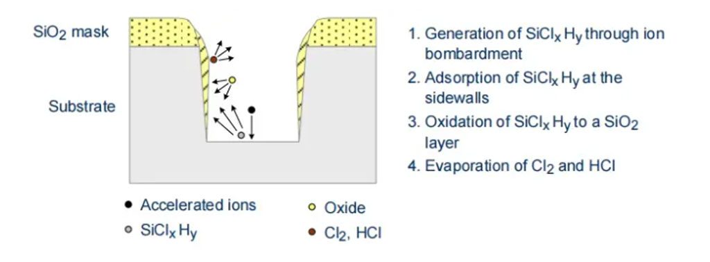
Increasing the pressure in the etching chamber reduces the average free path of the particles. Consequently, there are more collisions, and particles travel in different directions. This results in less directional etching, with the etching process gaining more chemical characteristics. Selectivity increases, and the etching profile becomes more isotropic. During silicon etching, anisotropic etching profiles are achieved by passivating the sidewalls. Thus, oxygen in the etching chamber reacts with the abraded silicon to form silicon dioxide, which deposits on vertical sidewalls. Due to ion bombardment, the oxide film on horizontal areas is removed, allowing lateral etching to continue.
Etch rate depends on pressure, high-frequency generator power, process gases, actual gas flow, and wafer temperature. Anisotropy increases with higher high-frequency power, lower pressure, and lower temperature. The uniformity of the etching process depends on the gases, the distance between the two electrodes, and the electrode material. If the distance is too small, the plasma cannot disperse uniformly, leading to non-uniformity. Increasing the distance between electrodes reduces the etch rate as the plasma spreads over a larger volume. Carbon has proven to be a preferred material for electrodes. Since fluorine and chlorine gases also attack carbon, electrodes produce a uniform strained plasma, so the wafer edges experience the same effects as the wafer center.
Selectivity and etch rate largely depend on the process gases. Fluorine and chlorine gases are mainly used for etching silicon and silicon compounds.
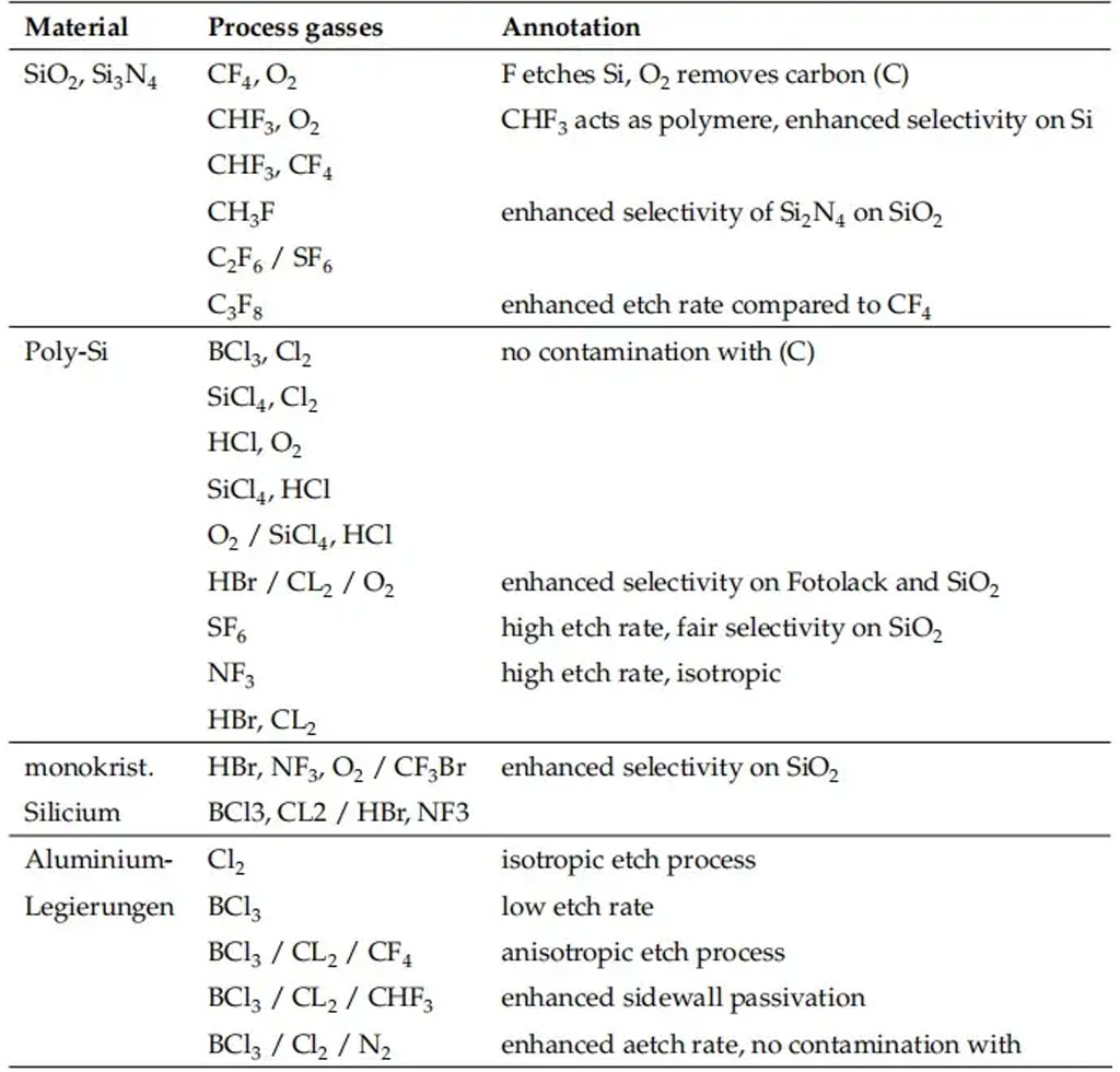
The etching process is not limited to a single gas, gas mixture, or fixed process parameters. For example, native oxide on polysilicon can first be removed at a high etch rate and low selectivity, followed by etching the polysilicon with higher selectivity relative to the underlying layer.