Etching, a subtractive manufacturing process widely employed in prototyping and design, involves the selective removal of material from a substrate using chemical or physical means. This technique has emerged as a cornerstone in the rapid development of prototypes across industries, including electronics, aerospace, automotive, and microfluidics. By leveraging etching, designers and engineers can accelerate the iteration of designs, refine concepts with precision, and transition from theoretical models to tangible products with remarkable efficiency. This article explores the principles, methodologies, applications, and advancements of etching in prototyping, with a focus on how it expedites the design process. Detailed comparisons of etching techniques, materials, and their impact on prototyping speed are provided to underscore the scientific and practical significance of this method.
Etching traces its origins to ancient practices of metalworking and artistry, where artisans used acidic solutions to engrave patterns onto copper and bronze surfaces. In the modern context, etching has evolved into a highly controlled, repeatable process integral to microfabrication and macro-scale prototyping. The advent of technologies such as photolithography, plasma etching, and laser-assisted etching has expanded its scope, enabling the creation of intricate features at scales ranging from nanometers to centimeters. For prototyping, where speed, accuracy, and adaptability are paramount, etching offers a unique combination of precision and scalability that distinguishes it from additive processes like 3D printing or traditional subtractive methods such as milling.
The fundamental mechanism of etching involves the application of an etchant—a chemical agent, plasma, or energy source—that selectively removes material from a substrate. Substrates can include metals (e.g., copper, aluminum, stainless steel), semiconductors (e.g., silicon), or polymers, depending on the prototyping requirements. The process typically begins with the preparation of the substrate, followed by the application of a protective mask or resist that defines the areas to be preserved. The etchant then interacts with the exposed regions, dissolving or ablating the material to form the desired pattern or structure. This sequence, while conceptually straightforward, encompasses a variety of techniques, each with distinct advantages in terms of speed, resolution, and material compatibility.
Wet Etching: A Chemical Approach to Rapid Prototyping
Wet etching, one of the earliest and most accessible forms of etching, relies on liquid chemical etchants to remove material. Commonly used etchants include acids (e.g., hydrochloric acid, nitric acid), bases (e.g., potassium hydroxide), and oxidizing agents (e.g., ferric chloride). The process is isotropic, meaning it etches uniformly in all directions, resulting in rounded or undercut features. For prototyping, wet etching is prized for its simplicity, low cost, and ability to process large batches of substrates simultaneously, making it a go-to method for initial design iterations.
In the context of electronics prototyping, wet etching is extensively used to fabricate printed circuit boards (PCBs). A typical workflow involves laminating a copper-clad substrate with a photoresist, exposing it to ultraviolet (UV) light through a photomask, and developing the resist to reveal the circuit pattern. The exposed copper is then etched away using ferric chloride or ammonium persulfate, leaving behind the conductive traces. This process, which can be completed in a matter of hours, allows engineers to quickly produce functional PCB prototypes for testing and validation. The speed of wet etching is further enhanced by its scalability; multiple boards can be etched in a single bath, reducing per-unit processing time.
However, wet etching has limitations that impact its suitability for certain prototyping applications. Its isotropic nature results in lower resolution compared to anisotropic methods, making it less ideal for features with high aspect ratios or submicron precision. Additionally, the handling and disposal of chemical etchants pose environmental and safety challenges, prompting the development of alternative techniques. Despite these drawbacks, wet etching remains a staple in prototyping due to its rapid setup and execution, particularly in educational settings and small-scale production environments.
Dry Etching: Precision and Control in Design Iteration
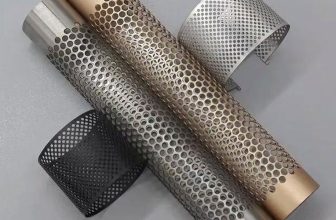
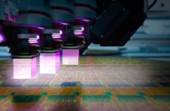
Dry etching, encompassing techniques such as plasma etching and reactive ion etching (RIE), represents a significant advancement over wet etching in terms of precision and control. Unlike wet etching, dry etching uses gaseous etchants or plasma to remove material, often in a vacuum chamber. This allows for anisotropic etching, where material is removed directionally, producing sharp, well-defined features. For prototyping applications requiring intricate geometries—such as microelectromechanical systems (MEMS) or integrated circuits (ICs)—dry etching offers unparalleled accuracy and repeatability.
Plasma etching, a subset of dry etching, employs a plasma—a partially ionized gas containing reactive species such as fluorine or chlorine—to etch the substrate. The process begins with the application of a mask, typically made of photoresist or a hard material like silicon dioxide, followed by exposure to the plasma. The reactive species bombard the substrate, chemically reacting with the exposed material and volatilizing it into gaseous byproducts that are evacuated from the chamber. This method’s directional control is enhanced in RIE, where an electric field accelerates ions toward the substrate, increasing the etch rate and enabling vertical sidewalls.
The speed of dry etching in prototyping lies in its ability to produce high-fidelity prototypes in a single step, reducing the need for multiple iterations. For example, in MEMS prototyping, a silicon wafer can be etched to form microstructures such as cantilevers or channels within minutes, depending on the etch depth and plasma parameters. This rapid turnaround is critical in design optimization, where engineers must test multiple configurations to refine performance. Moreover, dry etching’s compatibility with semiconductor materials aligns with the demands of modern electronics, where miniaturization and integration are key drivers of innovation.
Despite its advantages, dry etching requires sophisticated equipment, such as plasma reactors, and precise control of parameters like gas composition, pressure, and power. These factors increase setup time and cost compared to wet etching, making it less practical for low-budget or preliminary prototyping. However, advancements in equipment design and process automation have mitigated these challenges, broadening dry etching’s accessibility to research labs and startups.
Laser Etching: Bridging Speed and Flexibility
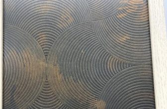
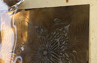
Laser etching, or laser ablation, introduces a non-contact approach to material removal, leveraging focused laser beams to vaporize or melt substrate regions. This technique spans a wide range of prototyping applications, from microscale features in semiconductors to macroscale patterns in metals and polymers. The speed of laser etching stems from its direct-write capability; unlike chemical etching, which requires masking and bath preparation, laser etching can begin immediately upon design upload to the system.
In prototyping, laser etching excels in producing custom parts with minimal lead time. For instance, a designer can create a digital model of a component—such as a microfluidic channel or a decorative panel—and use a laser system to etch the pattern into a substrate within minutes. The process’s flexibility is enhanced by the variety of laser types available, including CO2 lasers for polymers and ceramics, Nd:YAG lasers for metals, and femtosecond lasers for ultra-precise microfabrication. Femtosecond lasers, in particular, minimize thermal damage by delivering energy in ultrashort pulses, preserving the integrity of surrounding material.
The speed of laser etching is further amplified by its compatibility with computer-aided design (CAD) software, enabling seamless integration into rapid prototyping workflows. Iterative design cycles benefit from this synergy, as modifications to a digital file can be immediately reflected in the etched prototype without retooling or mask fabrication. However, laser etching’s throughput is limited by its sequential nature; unlike wet etching’s batch processing, it typically operates on a single substrate at a time. For high-volume prototyping, this can be a bottleneck, though multi-beam systems and automated stages are addressing this limitation.
Comparative Analysis of Etching Techniques
To elucidate the role of etching in speeding up design, a detailed comparison of wet etching, dry etching, and laser etching is essential. Each technique offers distinct trade-offs in terms of speed, resolution, cost, and material compatibility, influencing its applicability to specific prototyping scenarios. The following table summarizes key parameters:
| Parameter | Wet Etching | Dry Etching (RIE) | Laser Etching |
|---|---|---|---|
| Mechanism | Chemical dissolution | Plasma/ion bombardment | Laser ablation |
| Speed (Setup Time) | Low (minutes) | Moderate (hours) | Low (minutes) |
| Speed (Processing Time) | Fast (minutes per batch) | Moderate (minutes per wafer) | Fast (seconds to minutes) |
| Resolution | Moderate (microns) | High (nanometers) | High (microns to nanometers) |
| Anisotropy | Isotropic | Anisotropic | Anisotropic |
| Cost | Low (chemicals, simple equipment) | High (plasma reactors) | Moderate (laser systems) |
| Material Compatibility | Metals, semiconductors, glass | Semiconductors, some metals | Metals, polymers, ceramics |
| Batch Processing | Yes | Limited | No |
| Environmental Impact | High (chemical waste) | Moderate (gas emissions) | Low (minimal waste) |
This table highlights wet etching’s advantage in rapid batch processing, making it ideal for initial PCB prototypes where speed outweighs precision. Dry etching, with its superior resolution, suits advanced prototyping in MEMS and ICs, where design validation requires exacting standards. Laser etching, meanwhile, offers unmatched flexibility and turnaround time, catering to custom or one-off prototypes across diverse materials.
Material Considerations in Etching for Prototyping
The choice of substrate significantly influences etching speed and design outcomes. Metals like copper and aluminum are staples in wet etching for electronics, owing to their reactivity with common etchants and conductivity. Silicon, the backbone of microfabrication, is readily processed via dry etching using fluorine-based plasmas, enabling rapid prototyping of sensors and actuators. Polymers such as polyimide and PMMA (polymethyl methacrylate) are increasingly etched with lasers for flexible electronics and microfluidics, leveraging their low cost and ease of patterning.
Etching rates, a critical factor in prototyping speed, vary by material and technique. For instance, copper etches at approximately 1–2 μm/min in ferric chloride, while silicon can achieve rates of 1–10 μm/min in RIE with SF6 plasma. Laser etching rates depend on power and material absorption; a 50W CO2 laser might ablate PMMA at 100 μm/s. These rates dictate the feasibility of producing a prototype within a given timeframe, balancing throughput with feature complexity.
Applications in Industry and Research
Etching’s role in speeding up design is evident across multiple domains. In electronics, PCB prototyping via wet etching enables rapid testing of circuit layouts, reducing development cycles from weeks to days. In MEMS, dry etching facilitates the creation of prototypes for accelerometers and gyroscopes, accelerating their integration into consumer devices. Laser etching, meanwhile, supports the aerospace industry by producing lightweight, intricate components for wind tunnel models, where turnaround time is critical for iterative testing.
In academic research, etching underpins the exploration of novel devices. Microfluidic prototyping, for instance, relies on etching to create channels and reservoirs in glass or polymer substrates, enabling rapid validation of lab-on-chip concepts. The ability to iterate designs quickly fosters innovation, as researchers can test hypotheses and refine systems without prolonged delays.
Advancements and Future Directions
Recent innovations in etching technology continue to enhance its utility in prototyping. Hybrid approaches, such as combining laser etching with wet etching, offer multi-scale patterning capabilities, speeding up the production of complex prototypes. Machine learning is also being integrated into dry etching processes, optimizing plasma parameters in real-time to maximize etch uniformity and rate. These developments promise to further compress design timelines, aligning with the accelerating pace of technological advancement.
Sustainability is another frontier, with efforts to reduce the environmental footprint of etching. Green etchants, such as hydrogen peroxide-based solutions, are gaining traction in wet etching, while dry etching systems are adopting closed-loop gas recycling. Laser etching, inherently low-waste, is poised to dominate eco-conscious prototyping workflows.
Conclusion
Etching, in its various forms, stands as a pivotal technique for speeding up design in prototyping. By offering rapid material removal, high precision, and adaptability to diverse substrates, it bridges the gap between concept and realization. Wet etching provides an accessible entry point for quick iterations, dry etching delivers the finesse required for cutting-edge applications, and laser etching marries speed with customization. As industries and researchers push the boundaries of innovation, etching’s evolution will continue to drive efficiency, ensuring that prototypes—and the designs they embody—reach fruition faster than ever before.