Etching is a critical process used across various industries, including microelectronics, metallurgy, art, and material science, to selectively remove material from a substrate to create patterns, designs, or functional surfaces. The duration of the etching process is highly variable, depending on factors such as the etching technique, the material being etched, the etchant used, the desired etch depth, and environmental conditions. This article provides a comprehensive examination of the etching process, exploring the factors that influence its duration, the types of etching techniques, and their applications. By delving into the scientific principles, practical considerations, and technological advancements, this article aims to offer a thorough understanding of how long the etching process takes in different contexts.
Etching is a subtractive manufacturing process that involves the selective removal of material from a solid surface, typically through chemical, physical, or electrochemical means. The process is employed in a wide range of applications, from creating intricate microchip circuits in semiconductor manufacturing to producing detailed engravings in art. The time required for etching varies significantly based on the method and the specific requirements of the task. For instance, wet chemical etching may take seconds to minutes, while dry etching processes, such as reactive ion etching (RIE), can range from minutes to hours, depending on the material and etch depth.
The etching process generally involves the application of an etchant—a substance or energy source that removes material from the substrate. The substrate is often protected by a mask, which defines the areas to be etched. The mask can be a resist (in semiconductor manufacturing), a metal stencil (in art), or another material resistant to the etchant. The etching duration is influenced by the rate at which the etchant interacts with the substrate, the thickness of the material to be removed, and external factors such as temperature and pressure.
This article is structured to provide a detailed analysis of etching durations across various techniques, with sections dedicated to wet etching, dry etching, electrochemical etching, and specialized methods like laser etching. Each section includes discussions of the underlying mechanisms, factors affecting etch time, and practical examples. Comparative tables are provided to summarize key data, enabling readers to understand the relative time requirements of different etching processes.
Wet Chemical Etching
Principles of Wet Chemical Etching
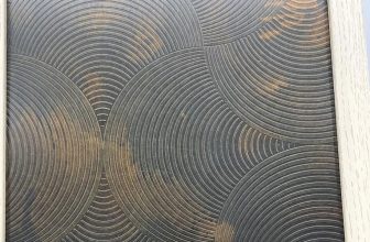
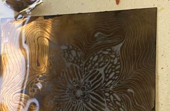
Wet chemical etching is one of the oldest and most widely used etching techniques, relying on liquid chemical solutions to remove material from a substrate. The process involves immersing the substrate in an etchant solution or applying the etchant to the surface. The etchant reacts chemically with the exposed material, dissolving it and leaving behind the desired pattern. Common etchants include acids (e.g., hydrochloric acid, nitric acid), bases (e.g., potassium hydroxide), and specialized solutions tailored to specific materials.
The duration of wet chemical etching depends on several factors, including the etchant concentration, the material’s chemical reactivity, the temperature of the solution, and the desired etch depth. For example, etching silicon with a potassium hydroxide (KOH) solution at 80°C may proceed at a rate of approximately 1 micrometer per minute, meaning a 10-micrometer-deep etch would take about 10 minutes. In contrast, etching copper with ferric chloride may occur at a faster rate, often completing in seconds for thin layers.
Factors Affecting Wet Etching Duration
- Etchant Concentration: Higher concentrations typically increase the etch rate, reducing the time required. However, excessively high concentrations may lead to uncontrolled etching or mask degradation.
- Temperature: Elevated temperatures accelerate chemical reactions, increasing the etch rate. For instance, raising the temperature of a KOH solution from 60°C to 80°C can double the etch rate for silicon.
- Material Properties: The crystal structure and composition of the substrate influence etch rates. Anisotropic etching of silicon, for example, is faster along certain crystallographic planes (e.g., <100> vs. <111>).
- Agitation: Stirring or agitating the etchant solution ensures a fresh supply of reactants at the surface, preventing depletion and maintaining a consistent etch rate.
- Mask Integrity: The mask must withstand the etchant for the entire duration. If the mask degrades, unwanted areas may be etched, affecting precision and requiring additional time for rework.
Applications and Time Estimates
Wet chemical etching is widely used in semiconductor manufacturing, printed circuit board (PCB) production, and metal engraving. In semiconductor fabrication, wet etching is employed to create features such as trenches or vias in silicon wafers. For a typical 5-micrometer-deep trench in silicon using a hydrofluoric acid (HF)-based etchant, the process may take 2–5 minutes, depending on the solution’s concentration and temperature.
In PCB manufacturing, copper is etched using ferric chloride or ammonium persulfate. A 35-micrometer-thick copper layer on a PCB may be etched in 5–10 minutes with ferric chloride at room temperature. In contrast, artistic etching of metals like zinc or copper for printmaking may take 10–30 minutes, as the process prioritizes precision over speed.
Table 1: Wet Chemical Etching Time Estimates
| Material | Etchant | Etch Depth (µm) | Temperature (°C) | Etch Rate (µm/min) | Time (min) |
|---|---|---|---|---|---|
| Silicon | KOH | 10 | 80 | 1.0 | 10 |
| Silicon | HF/Nitric Acid | 5 | 25 | 2.0 | 2.5 |
| Copper | Ferric Chloride | 35 | 25 | 5.0 | 7 |
| Aluminum | Phosphoric Acid | 2 | 40 | 0.5 | 4 |
| Zinc | Nitric Acid | 50 | 20 | 2.5 | 20 |
Note: Etch rates and times are approximate and depend on specific conditions.
Dry Etching
Principles of Dry Etching
Dry etching encompasses a family of etching techniques that use gases or plasmas to remove material, offering greater precision and control compared to wet etching. Common dry etching methods include reactive ion etching (RIE), plasma etching, and ion beam etching. These techniques are essential in microelectronics, where sub-micrometer features are required.
In dry etching, a plasma is generated by applying radiofrequency (RF) energy to a gas mixture, creating reactive species (ions, radicals) that interact with the substrate. The etching process can be isotropic (uniform in all directions) or anisotropic (directional), depending on the technique and parameters. The duration of dry etching is influenced by the plasma chemistry, power, pressure, and substrate material.
Factors Affecting Dry Etching Duration
- Plasma Chemistry: The choice of gas (e.g., SF₆ for silicon, Cl₂ for aluminum) determines the etch rate. Fluorine-based plasmas etch silicon faster than chlorine-based plasmas etch metals.
- Power and Pressure: Higher RF power increases the density of reactive species, accelerating etching. Lower pressure enhances anisotropy but may reduce the etch rate.
- Substrate Material: Materials with strong chemical bonds (e.g., silicon dioxide) etch more slowly than those with weaker bonds (e.g., photoresist).
- Mask Selectivity: The mask must resist the plasma. A low selectivity ratio (etch rate of substrate vs. mask) requires thicker masks, potentially increasing process time.
- Chamber Conditions: Contamination or residue buildup in the etching chamber can slow the process, necessitating cleaning cycles.
Applications and Time Estimates
Dry etching is the cornerstone of modern semiconductor manufacturing, used to define features in integrated circuits. For example, etching a 0.5-micrometer-deep trench in silicon using SF₆-based RIE may take 1–3 minutes, with an etch rate of 0.2–0.5 micrometers per minute. Etching silicon dioxide (SiO₂) with a CHF₃ plasma is slower, often requiring 5–10 minutes for a 1-micrometer depth due to the material’s chemical stability.
In microelectromechanical systems (MEMS) fabrication, deep reactive ion etching (DRIE) is used to create high-aspect-ratio structures in silicon. A 100-micrometer-deep trench may take 30–60 minutes, depending on the Bosch process parameters, which alternate etching and passivation cycles.
Table 2: Dry Etching Time Estimates
| Material | Etching Method | Etch Depth (µm) | Gas Chemistry | Etch Rate (µm/min) | Time (min) |
|---|---|---|---|---|---|
| Silicon | RIE | 0.5 | SF₆/O₂ | 0.3 | 1.7 |
| Silicon Dioxide | RIE | 1.0 | CHF₃/Ar | 0.15 | 6.7 |
| Aluminum | Plasma Etching | 0.2 | Cl₂/BCl₃ | 0.1 | 2.0 |
| Silicon | DRIE (Bosch) | 100 | SF₆/C₄F₈ | 2.0 | 50 |
| Gallium Arsenide | RIE | 0.3 | Cl₂/Ar | 0.2 | 1.5 |
Note: Etch rates and times are approximate and depend on equipment and conditions.
Electrochemical Etching
Principles of Electrochemical Etching
Electrochemical etching, also known as anodic etching, involves the use of an electric current to drive material removal in an electrolyte solution. The substrate acts as the anode, and a counter electrode (cathode) completes the circuit. The electrolyte facilitates ion transfer, enabling selective material dissolution. This method is commonly used for metals, semiconductors, and porous material fabrication.
The duration of electrochemical etching depends on the current density, electrolyte composition, and material properties. For example, porous silicon formation via anodic etching in an HF-based electrolyte may take 10–60 minutes, depending on the desired porosity and thickness.
Factors Affecting Electrochemical Etching Duration
- Current Density: Higher current densities increases the etch rate but may lead to uneven etching or surface defects.
- Electrolyte Composition: The concentration of active species (e.g., HF for silicon) affects the etch rate and surface morphology.
- Material Conductivity: Highly conductive materials etch faster due to efficient charge transfer.
- Temperature: Elevated temperatures can enhance ion mobility, reducing etching time.
- Electrode Configuration: The distance and geometry of the electrodes influence current distribution and etch uniformity.
Applications and Time Estimates
Electrochemical etching is used in applications such as porous silicon fabrication for sensors, metal surface texturing, and electropolishing. For instance, creating a 50-micrometer-thick porous silicon layer may take 20–40 minutes at a current density of 10–50 mA/cm². Electropolishing stainless steel to achieve a smooth surface may require 5–15 minutes, depending on the electrolyte (e.g., sulfuric acid-phosphoric acid mixture) and current.
Table 3: Electrochemical Etching Time Estimates
| Material | Electrolyte | Etch Depth (µm) | Current Density (mA/cm²) | Etch Rate (µm/min) | Time (min) |
|---|---|---|---|---|---|
| Silicon | HF/Ethanol | 50 | 20 | 2.0 | 25 |
| Stainless Steel | H₂SO₄/H₃PO₄ | Surface | 100 | N/A (Polishing) | 10 |
| Aluminum | HCl/NaCl | 10 | 50 | 1.0 | 10 |
| Titanium | H₂SO₄/Methanol | 5 | 30 | 0.5 | 10 |
| Copper | HNO₃/Ethanol | 20 | 40 | 1.5 | 13.3 |
Note: Etch rates and times are approximate and depend on specific conditions.
Laser Etching
Principles of Laser Etching
Laser etching, or laser ablation, uses focused laser beams to remove material through vaporization, melting, or chemical reactions. The process is highly precise, enabling intricate patterns without the need for masks. The duration of laser etching depends on the laser power, wavelength, pulse duration, and material properties.
Factors Affecting Laser Etching Duration
- Laser Power and Pulse Duration: Higher power and shorter pulses increase the ablation rate, reducing etching time.
- Material Properties: Materials with lower melting points or higher absorption at the laser wavelength etch faster.
- Scan Speed: Faster scanning reduces processing time but may compromise precision.
- Etch Depth: Deeper etches require multiple passes, increasing total time.
- Beam Focus: A tightly focused beam enhances efficiency, minimizing time.
Applications and Time Estimates
Laser etching is used in microfabrication, marking, and artistic engraving. For example, etching a 10-micrometer-deep pattern in stainless steel with a 50-watt fiber laser may take 1–5 seconds per square centimeter, depending on the scan speed. Engraving a 0.1-mm-deep logo on glass may require 10–20 seconds for a 5 cm² area.
Table 4: Laser Etching Time Estimates
| Material | Laser Type | Etch Depth (µm) | Power (W) | Scan Speed (mm/s) | Time (s/cm²) |
|---|---|---|---|---|---|
| Stainless Steel | Fiber | 10 | 50 | 1000 | 2 |
| Glass | CO₂ | 100 | 40 | 500 | 15 |
| Silicon | Nd:YAG | 5 | 20 | 800 | 3 |
| Aluminum | Fiber | 20 | 30 | 1200 | 1.5 |
| Polymer | UV Laser | 50 | 10 | 600 | 5 |
Note: Times are approximate and depend on equipment and settings.
Comparison of Etching Techniques
The choice of etching technique depends on the application, material, and desired precision. Wet etching is cost-effective and suitable for large-scale features but lacks the precision of dry etching. Dry etching offers high anisotropy and resolution, making it ideal for microelectronics. Electrochemical etching is effective for porous materials and surface finishing, while laser etching excels in maskless, high-speed applications.
Table 5: Comparison of Etching Techniques
| Technique | Typical Materials | Etch Rate (µm/min) | Precision | Time Range | Cost | Applications |
|---|---|---|---|---|---|---|
| Wet Etching | Si, Cu, Al, Zn | 0.5–5.0 | Moderate | Seconds–Minutes | Low | PCBs, Art |
| Dry Etching | Si, SiO₂, GaAs | 0.1–2.0 | High | Minutes–Hours | High | Semiconductors, MEMS |
| Electrochemical | Si, Stainless Steel | 0.5–2.0 | Moderate | Minutes | Medium | Porous Si, Polishing |
| Laser Etching | Metals, Glass, Polymers | 1–100 (µm/s) | High | Seconds–Minutes | High | Marking, Microfabrication |
Advanced Considerations
Etch Uniformity and Process Control
Achieving uniform etching across a substrate is critical, particularly in large-scale manufacturing. Non-uniform etching can result from variations in etchant concentration, plasma density, or laser intensity. Process control techniques, such as real-time monitoring and feedback systems, help maintain consistent etch rates and reduce variability in etching time.
Environmental and Safety Factors
Etching processes often involve hazardous chemicals, high-energy plasmas, or lasers, requiring strict safety protocols. Wet etching generates chemical waste, necessitating proper disposal. Dry etching produces gaseous byproducts, requiring exhaust systems. Laser etching may produce fumes or debris, requiring ventilation. These factors can indirectly affect etching time by imposing setup or cleanup requirements.
Technological Advancements
Recent advancements have reduced etching times while improving precision. For example, atomic layer etching (ALE) enables precise, layer-by-layer material removal, with cycle times of seconds per layer. Machine learning is being integrated into etching systems to optimize parameters, reducing trial-and-error and minimizing process duration.
Conclusion
The duration of the etching process is highly context-dependent, ranging from seconds for laser etching to hours for deep dry etching. By understanding the principles, factors, and applications of each technique, practitioners can select the most appropriate method for their needs. Wet etching offers simplicity and speed for less precise applications, while dry etching provides the resolution required for advanced microelectronics. Electrochemical and laser etching offer specialized capabilities for specific materials and patterns. The provided tables summarize key data, enabling comparisons across techniques. As technology advances, etching processes are becoming faster, more precise, and more environmentally sustainable, broadening their impact across industries.