Lamination, in the context of etching parts, refers to the process of applying a protective or masking layer to a substrate—typically a metal or other material—prior to subjecting it to an etching process. This technique is widely utilized in manufacturing, prototyping, and artistic applications to selectively remove material from specific areas while preserving others. Etching itself is a subtractive fabrication method, where chemical, mechanical, or electrochemical means are employed to erode material, leaving behind intricate patterns, designs, or functional features. Lamination serves as a critical preparatory step, ensuring precision and protecting regions of the workpiece that must remain intact.
The practice of lamination for etching has evolved significantly, with roots tracing back to early printmaking and metalworking techniques. Today, it is a cornerstone of industries such as electronics, aerospace, and jewelry-making, where precision components like circuit boards, gears, or decorative elements are produced. The lamination process involves adhering a resistant film—often a polymer, photoresist, or adhesive-backed material—to the substrate, which is then selectively removed or altered to expose areas for etching. This article explores the methodologies, materials, tools, and considerations involved in lamination for etching parts, providing a comprehensive guide for practitioners and enthusiasts alike.
Historical Context of Lamination in Etching
The concept of lamination as a precursor to etching can be traced to the medieval art of printmaking, where artisans applied waxes or resins to metal plates to protect certain areas from acid baths. By the 19th century, the industrial revolution spurred advancements in chemical etching, particularly for producing detailed engravings and machinery components. Lamination techniques grew more sophisticated with the advent of photography and photolithography in the 20th century, enabling the use of light-sensitive films for precision masking. The electronics industry, in particular, revolutionized lamination with the development of dry film photoresists, which remain a standard in printed circuit board (PCB) manufacturing.
Historically, lamination was a manual process, relying on skilled labor to apply and pattern masking materials. Modern methods, however, leverage automation, advanced adhesives, and digital design tools, making the process accessible to hobbyists and professionals alike. Understanding this evolution provides context for the diverse approaches to lamination available today, from traditional wax-based methods to cutting-edge laser-patterned films.
Fundamental Principles of Lamination for Etching
At its core, lamination for etching involves creating a barrier that resists the etchant—typically an acid, base, or plasma—used to remove material from the substrate. The laminate must adhere uniformly to the surface, withstand the etching conditions, and be removable or modifiable to expose the desired pattern. This requires a balance of material properties, including adhesion strength, chemical resistance, and ease of patterning.
The substrate, often a metal such as copper, steel, or aluminum, dictates the choice of laminate and etchant. For instance, copper etching for PCBs commonly employs ferric chloride, necessitating a laminate that resists this corrosive solution. The laminate itself may be a liquid photoresist applied via spin-coating, a dry film rolled onto the surface, or even a simple adhesive vinyl cut to shape. Each method has distinct advantages, depending on the scale, complexity, and precision required for the etched part.
Materials Used in Lamination for Etching
Substrates
The choice of substrate is foundational to the lamination and etching process. Common materials include:
- Copper: Widely used in electronics for its conductivity and etchability.
- Steel: Employed in mechanical parts and decorative items, requiring robust laminates to resist strong etchants like nitric acid.
- Aluminum: Lightweight and corrosion-resistant, often etched for aerospace components.
- Glass: Used in specialized applications, such as microfluidic devices, with plasma or hydrofluoric acid etching.
Laminates
Laminates vary in composition and application method:
- Photoresists: Light-sensitive polymers, available as liquid (e.g., SU-8) or dry film (e.g., Dupont Riston). They are patterned using UV light and a mask or direct laser writing.
- Adhesive Films: Vinyl or polyester tapes, manually cut or plotted, suitable for simple designs.
- Waxes and Resins: Traditional options, applied by hand or heated, offering flexibility for artistic etching.
- Thermal Laminates: Polymer films activated by heat and pressure, common in industrial settings.
Etchants
The etchant must be compatible with both the substrate and laminate:
- Ferric Chloride: Standard for copper etching, moderately aggressive.
- Nitric Acid: Effective for steel and other metals, requiring durable laminates.
- Hydrofluoric Acid: Used for glass, highly hazardous, and necessitating specialized resists.
- Plasma: A dry etching method for semiconductors, compatible with photoresists.
Tools and Equipment for Lamination
Effective lamination requires a suite of tools tailored to the chosen method:
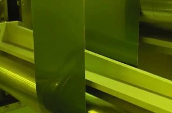
- Laminators: Roller-based machines that apply dry film photoresists with heat and pressure, ensuring bubble-free adhesion.
- UV Exposure Units: Essential for photoresist patterning, delivering controlled light doses through masks.
- Cutting Tools: Manual knives, plotters, or laser cutters for shaping adhesive films.
- Spin Coaters: Used to apply liquid photoresists evenly across a substrate.
- Cleaning Stations: Ultrasonic baths or solvent tanks to prepare surfaces by removing oils and debris.
Industrial settings may employ automated systems integrating these tools, while hobbyists often rely on affordable alternatives like handheld rollers or DIY exposure boxes.
Step-by-Step Process of Lamination for Etching
Surface Preparation
The substrate must be pristine to ensure laminate adhesion. This involves:
- Cleaning: Remove grease, oxides, and particulates using solvents (e.g., acetone) or abrasive pads.
- Degreasing: Apply a degreaser like isopropyl alcohol to eliminate residual oils.
- Drying: Air-dry or use a heat gun to prevent moisture interference.
Applying the Laminate
The application method depends on the laminate type:
- Dry Film Photoresist:
- Cut the film to size, slightly larger than the substrate.
- Peel off one protective layer and align the film with the substrate.
- Feed the assembly through a laminator at the recommended temperature (typically 100–120°C).
- Trim excess film and inspect for air bubbles or wrinkles.
- Liquid Photoresist:
- Place the substrate on a spin coater.
- Dispense the resist and spin at 1000–3000 RPM for uniform thickness (e.g., 1–10 micrometers).
- Bake the coated substrate (e.g., 90°C for 10 minutes) to cure the resist.
- Adhesive Film:
- Cut the design using a plotter or manually with a stencil.
- Peel and stick the film onto the substrate, smoothing it with a roller.
Patterning the Laminate
Expose the design onto the laminate:
- Photolithography:
- Overlay a mask (printed transparency or chrome-on-glass) onto the photoresist.
- Expose to UV light (e.g., 365 nm for 10–60 seconds, depending on resist sensitivity).
- Develop the resist in a chemical bath (e.g., sodium carbonate for positive resists) to reveal the pattern.
- Manual Cutting: For adhesive films, remove unwanted areas with a scalpel or peel away pre-cut sections.
- Laser Ablation: Use a laser to burn away specific laminate regions, ideal for precision work.
Etching the Substrate
Immerse or treat the patterned substrate:
- Prepare the etchant (e.g., dilute ferric chloride to 40% concentration).
- Submerge the substrate in an etching tank or apply etchant with a sponge for controlled areas.
- Agitate gently to ensure even material removal (etch times vary: 5–30 minutes for copper).
- Monitor progress and remove when the desired depth is achieved.
Laminate Removal
Strip the remaining laminate:
- Chemical Stripping: Use acetone or a proprietary stripper for photoresists.
- Mechanical Peeling: Peel off adhesive films by hand or with tweezers.
- Cleaning: Rinse the etched part with water or solvent to remove residue.
Advanced Techniques in Lamination for Etching
Multilayer Lamination
For complex parts, multiple laminate layers may be applied:
- Stack resists with varying sensitivities to create stepped etch depths.
- Use intermediate etching steps to expose deeper layers selectively.
Double-Sided Etching
For substrates like PCBs:
- Laminate both sides with aligned patterns.
- Etch simultaneously in a vertical tank to ensure uniformity.
Laser-Assisted Lamination
Lasers enhance precision by:
- Directly patterning photoresists without masks.
- Cutting adhesive films with sub-millimeter accuracy.
Safety Considerations
Lamination and etching involve hazardous materials:
- Ventilation: Work in a fume hood or well-ventilated area to avoid inhaling etchant vapors.
- Protective Gear: Wear gloves, goggles, and aprons to shield against splashes.
- Disposal: Neutralize and dispose of etchants per local regulations (e.g., neutralize acids with baking soda).
Applications of Lamination and Etching
Electronics
PCBs rely on lamination to define conductive traces, with etched copper forming circuits.
Mechanical Engineering
Precision gears, shims, and springs are etched from metal sheets, often for aerospace or automotive use.
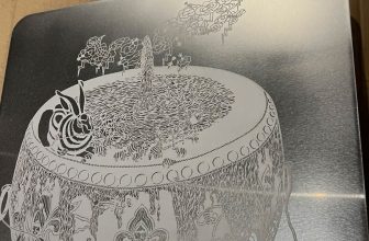
Art and Jewelry
Etched metal plates or pendants showcase intricate designs, blending craftsmanship with technical skill.
Comparison of Lamination Methods
| Method | Material Cost | Precision | Ease of Use | Typical Use Case | Equipment Needed |
|---|---|---|---|---|---|
| Dry Film Photoresist | Moderate | High | Moderate | PCB manufacturing | Laminator, UV unit, developer |
| Liquid Photoresist | High | Very High | Difficult | Microfabrication | Spin coater, oven, UV unit |
| Adhesive Vinyl | Low | Low | Easy | Hobbyist etching, art | Plotter or knife, roller |
| Wax/Resin | Very Low | Low | Moderate | Traditional metal etching | Brush, heat source |
| Thermal Laminate | Moderate | High | Moderate | Industrial parts | Thermal laminator |
Troubleshooting Common Issues
- Poor Adhesion: Ensure thorough cleaning and proper lamination pressure/temperature.
- Underexposure: Increase UV dose or check mask alignment.
- Overetching: Reduce etch time or dilute the etchant.
- Bubbles/Wrinkles: Use a roller or slower lamination speed.
Conclusion
Innovations include:
- Nanomaterial Resists: Enhancing resolution for microscale etching.
- Eco-Friendly Etchants: Replacing harsh chemicals with biodegradable alternatives.
- Automation: Fully integrated systems for mass production.
Lamination for etching parts is a versatile and precise process, bridging art, science, and engineering. By mastering its stages—from material selection to patterning and etching—practitioners can produce components with unparalleled detail. As technology advances, the techniques and tools will continue to evolve, broadening the scope of what’s possible in etched part fabrication.