Laminating metal sheets with photoresistant films is a sophisticated process widely utilized in various industries, including electronics, microfabrication, and printed circuit board (PCB) manufacturing. This technique involves the application of a light-sensitive polymer film, known as a photoresist, onto a metal substrate to enable precise patterning through photolithography. The process is critical for creating intricate designs, such as circuits or microstructures, by selectively exposing the photoresist to light and subsequently developing it to reveal the desired pattern. This article provides a comprehensive exploration of the methods, materials, equipment, and scientific principles involved in laminating metal sheets with photoresistant films, offering a detailed guide for researchers, engineers, and practitioners.
Historical Context and Development
The practice of laminating metal sheets with photoresistant films emerged as a cornerstone of modern microfabrication technology in the mid-20th century. The development of photoresists can be traced back to the 1950s, when the burgeoning semiconductor industry sought methods to miniaturize electronic components. Early photoresists were liquid-based, applied via spin-coating techniques, but these methods proved challenging for large-scale or non-planar substrates like metal sheets. The introduction of dry film photoresists in the 1960s, pioneered by companies such as DuPont with their Riston product line, revolutionized the field. Dry film photoresists offered a uniform, pre-manufactured layer that could be laminated onto metal surfaces, simplifying the process and improving consistency.
The evolution of this technology has been driven by the demand for higher resolution, greater durability, and compatibility with diverse substrates. Today, laminating metal sheets with photoresistant films is a standard procedure in PCB fabrication, where copper-clad laminates are patterned to create electrical circuits, and in microelectromechanical systems (MEMS), where precise etching of metal surfaces is required. The process has also found applications in aerospace, automotive, and medical device manufacturing, reflecting its versatility and importance in modern engineering.
Scientific Principles of Photoresistant Films
Photoresistant films are polymers that undergo a chemical change when exposed to light, typically ultraviolet (UV) radiation. This property, known as photosensitivity, allows them to serve as a mask for subsequent processing steps, such as etching or deposition. Photoresists are classified into two main types: positive and negative. Positive photoresists become soluble in a developer solution upon exposure to light, while negative photoresists become insoluble, cross-linking to form a stable structure. For laminating metal sheets, negative dry film photoresists are often preferred due to their robustness and ease of application over large areas.
The chemical composition of photoresistant films typically includes a polymer base, a photoactive compound (PAC), and a solvent or carrier medium (in liquid forms). In dry film photoresists, the polymer is pre-formed into a solid sheet, sandwiched between protective layers of polyethylene and polyester. The polymer base, often an acrylate or epoxy, provides mechanical strength, while the PAC, such as diazonaphthoquinone (DNQ) in positive resists or a cross-linking agent in negative resists, enables the photochemical reaction. When UV light strikes the film, it triggers a chain reaction—either breaking bonds in positive resists or forming new bonds in negative resists—altering the film’s solubility.
The lamination process relies on adhesion between the photoresist and the metal surface, governed by intermolecular forces such as van der Waals interactions and, in some cases, chemical bonding. Surface preparation of the metal sheet is critical to ensure strong adhesion, as contaminants or oxides can weaken the interface. The application of heat and pressure during lamination enhances this adhesion by promoting polymer flow and contact with the metal substrate.
Materials Used in Lamination
Metal Substrates
The choice of metal sheet is dictated by the intended application. Copper is the most common substrate in PCB manufacturing due to its excellent electrical conductivity and compatibility with etching processes. Aluminum, stainless steel, and titanium are also used, particularly in applications requiring corrosion resistance or lightweight properties. The thickness of the metal sheet typically ranges from 0.1 mm to 2 mm, depending on structural requirements and processing constraints.
Photoresistant Films
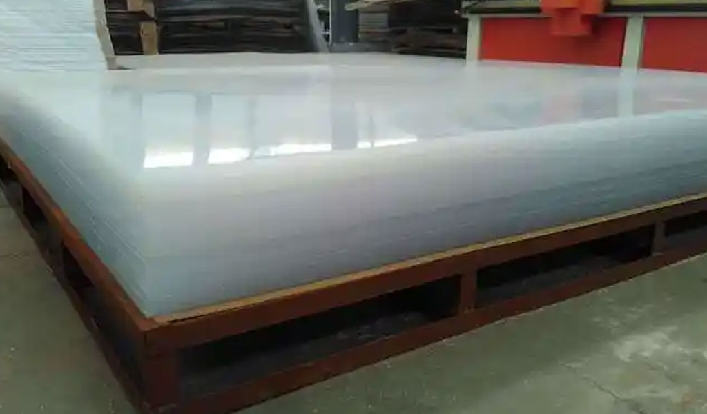
Dry film photoresists are available in various formulations, each tailored to specific needs. Common commercial products include DuPont Riston, Ordyl P-50100, and Tokyo Ohka Kogyo’s TMMF S2000. These films vary in thickness (typically 15–100 µm), sensitivity to UV wavelengths, and resolution capabilities. For example, Riston 4615 offers a thickness of 38 µm and is widely used for fine-line PCB patterns, while thicker films like Ordyl P-50100 (up to 200 µm with multilayer lamination) are suited for high-aspect-ratio structures in MEMS.
The structure of a dry film photoresist consists of three layers: a polyethylene separation sheet, the photoresist layer, and a polyester support film. The polyethylene layer protects the photoresist during storage and is removed before lamination, while the polyester film provides mechanical support and is peeled off after exposure.
Adhesives and Surface Treatments
While dry film photoresists are inherently adhesive when heated, some applications may require additional surface treatments to enhance bonding. Chemical etching, sandblasting, or anodizing can increase surface roughness and energy, improving adhesion. For instance, phosphoric acid anodizing of aluminum creates a porous oxide layer that interlocks with the photoresist, strengthening the interface.
Equipment for Lamination
Laminators
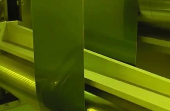
The lamination process requires specialized equipment to apply heat and pressure uniformly across the metal sheet. Hot roll laminators are the most common, featuring heated rollers that press the photoresist onto the substrate as it passes through. Typical operating temperatures range from 50°C to 120°C, with roller pressures of 0.5–2 MPa. Examples include the Think & Tinker LamiLam 3200 and industrial-scale machines from Burkle.
UV Exposure Units
After lamination, the photoresist is exposed to UV light through a photomask to define the pattern. Exposure units vary from simple benchtop devices with mercury vapor lamps (emitting at 365–405 nm) to sophisticated collimated light sources for high-resolution work. Exposure doses typically range from 100–500 mJ/cm², depending on the photoresist’s sensitivity.
Developers and Etchants
Post-exposure development removes unexposed (negative resist) or exposed (positive resist) areas using chemical solutions, such as sodium carbonate for negative resists or potassium hydroxide for positive resists. Etching then transfers the pattern into the metal, often using ferric chloride for copper or hydrofluoric acid for other metals.
Step-by-Step Lamination Process
Surface Preparation
The metal sheet must be meticulously cleaned to remove oils, oxides, and debris that could impair adhesion. A typical cleaning sequence involves:
- Degreasing: Immersion in a solvent like acetone or isopropyl alcohol.
- Mechanical Abrasion: Light sanding or brushing to increase surface roughness.
- Chemical Cleaning: Treatment with an acid (e.g., sulfuric acid) or alkaline solution to remove oxides.
- Rinsing and Drying: Deionized water rinse followed by air drying or baking at 100°C to eliminate moisture.
Film Application
The dry film photoresist is applied as follows:
- Peeling the Protective Layer: The polyethylene separation sheet is removed, exposing the adhesive side of the photoresist.
- Alignment: The film is carefully aligned with the metal sheet, often using a jig or vacuum table to prevent wrinkles.
- Lamination: The metal sheet and film are fed into a hot roll laminator. The rollers, heated to 80–110°C, apply pressure (e.g., 1 MPa) to bond the film to the metal. The speed (typically 0.5–2 m/min) ensures uniform contact without overheating.
Exposure
The laminated sheet is placed under a UV exposure unit with a photomask aligned over the photoresist. The mask, a transparent film with opaque patterns, blocks light from certain areas. Exposure time varies (e.g., 10–30 seconds for a 200 mJ/cm² dose), depending on the light source and resist type. For negative resists, exposed areas cross-link and harden.
Development
The exposed film is immersed in a developer solution (e.g., 1% sodium carbonate at 30°C) for 1–5 minutes. Unexposed areas dissolve, revealing the metal beneath, while exposed areas remain as a protective mask. The sheet is then rinsed with water to stop the reaction.
Etching and Stripping
The metal is etched using an appropriate chemical (e.g., ferric chloride for copper, 30–60 minutes at 40°C), transferring the pattern into the substrate. After etching, the remaining photoresist is stripped using a stronger solution (e.g., 5% sodium hydroxide) or organic solvents like acetone, leaving the patterned metal sheet.
Optimization Techniques
Temperature and Pressure Control
Optimal lamination requires balancing temperature and pressure to avoid defects. Excessive heat (above 120°C) can liquefy the photoresist, causing sagging or channel clogging in microstructures, while insufficient pressure (<0.5 MPa) may result in poor adhesion. A slow heating rate (e.g., 2°C/min) minimizes thermal stress.
Multilayer Lamination
For thicker resists, multiple layers can be laminated sequentially. Each layer is applied, exposed, and developed before adding the next, enabling high-aspect-ratio patterns. This technique is common in LIGA (Lithographie, Galvanoformung, Abformung) processes for MEMS.
Alternative Methods
A novel water-based method, inspired by histological techniques, involves floating the photoresist on warm water to remove dust and ensure flatness before applying it to the metal. This approach, though less common, can reduce bubbles and improve uniformity.
Applications
Printed Circuit Boards
In PCB manufacturing, copper sheets laminated with photoresist are patterned to create conductive traces. The process supports fine-line resolutions (down to 25 µm) and is scalable for mass production.
Microelectromechanical Systems
MEMS devices, such as sensors and actuators, use laminated metal sheets to fabricate microstructures. Thick resists (e.g., 100 µm) enable deep etching for complex geometries.
Decorative and Functional Coatings
Beyond electronics, photoresist lamination can pattern metal sheets for aesthetic purposes (e.g., jewelry) or functional coatings (e.g., anti-corrosion layers).
Comparative Analysis
| Property | Positive Resist | Negative Resist |
|---|---|---|
| Mechanism | Becomes soluble on exposure | Becomes insoluble on exposure |
| Resolution | Higher (sub-micron) | Moderate (10–50 µm) |
| Thickness Range | 1–10 µm (liquid) | 15–200 µm (dry film) |
| Adhesion to Metal | Moderate | Strong |
| Common Use | Semiconductor fabrication | PCB, MEMS |
| Metal | Conductivity (S/m) | Corrosion Resistance | Typical Thickness (mm) | Applications |
|---|---|---|---|---|
| Copper | 5.96 × 10⁷ | Moderate | 0.1–1.0 | PCBs, electronics |
| Aluminum | 3.77 × 10⁷ | High | 0.2–2.0 | Aerospace, lightweight |
| Stainless Steel | 1.45 × 10⁶ | Very High | 0.5–2.0 | Medical devices |
| Titanium | 2.38 × 10⁶ | Very High | 0.3–1.5 | Biomedical, aerospace |
| Equipment | Temperature Range (°C) | Pressure Range (MPa) | Speed (m/min) | Applications |
|---|---|---|---|---|
| Hot Roll Laminator | 50–120 | 0.5–2.0 | 0.5–2.0 | PCB, large-scale |
| Vacuum Laminator | 40–100 | 0.1–1.0 | N/A | MEMS, precision |
| Manual Laminator | 60–110 | 0.5–1.5 | Manual | Prototyping, small-scale |
Conclusion
Advancements in photoresist chemistry, such as the development of biodegradable films, promise to reduce environmental impact. Innovations in lamination equipment, including automated alignment systems and real-time monitoring, could enhance precision and throughput. Additionally, integrating photoresist lamination with additive manufacturing techniques, such as 3D printing metal substrates, may open new avenues for hybrid fabrication.
Adhesion Issues
Poor adhesion, often due to surface contamination, can be mitigated by rigorous cleaning and surface treatments like plasma etching. Adjusting lamination parameters also helps.
Resolution Limits
The resolution of dry film photoresists (typically 10–50 µm) is lower than liquid resists (<1 µm). Using thinner films or advanced exposure systems (e.g., laser direct imaging) can improve precision.
Environmental Concerns
Chemical developers and etchants pose disposal challenges. Water-based developers and recyclable etchants (e.g., cupric chloride) offer greener alternatives.
Laminating metal sheets with photoresistant films is a multifaceted process that combines materials science, engineering, and photochemistry to achieve precise patterning on metal substrates. From its historical roots in semiconductor technology to its current applications in electronics and beyond, the technique has evolved into a reliable and versatile method. By understanding the scientific principles, optimizing process parameters, and addressing challenges, practitioners can harness its full potential. As technology progresses, this method will likely continue to play a pivotal role in advancing manufacturing capabilities across diverse fields.