Metal etching, a sophisticated and precise manufacturing process, has emerged as a cornerstone technique in the fabrication of intricate components for artificial intelligence (AI)-driven robots. This subtractive method involves the selective removal of material from a metal substrate using chemical, electrochemical, or physical means, leaving behind finely detailed patterns, structures, or functional features. Its application in crafting parts for AI robots—whose operations demand exceptional precision, durability, and complexity—has revolutionized the production of mechanical and electronic components. From microgears in robotic actuators to intricate circuit pathways in control systems, metal etching provides a versatile and reliable solution that meets the stringent requirements of modern robotics. This article explores the principles, methodologies, applications, and advancements of metal etching in the context of AI robot parts, delving into its scientific underpinnings, practical implementations, and future potential.
The origins of metal etching can be traced back to ancient practices, where artisans used rudimentary acids to engrave decorative patterns onto metal surfaces. However, its evolution into a high-precision industrial process began in the 20th century with the advent of photochemical machining (PCM), also known as chemical etching or photoetching. This technique, which relies on photolithography to define patterns on metal, has since become a staple in industries requiring microscale accuracy, such as aerospace, electronics, and, more recently, robotics. For AI robots, which integrate advanced sensors, processors, and mechanical systems, metal etching offers unparalleled control over feature size, shape, and material properties, enabling the production of components that are both lightweight and robust.
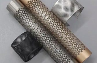
At its core, metal etching involves the use of a corrosive agent—typically an acid, base, or salt solution—to dissolve unprotected areas of a metal surface. The process begins with the selection of a metal substrate, which, in the context of AI robot parts, may include materials such as stainless steel, titanium, copper, aluminum, or specialized alloys like Inconel or Kovar. These metals are chosen based on their mechanical strength, corrosion resistance, electrical conductivity, or thermal stability, all of which are critical to the performance of robotic systems. For instance, stainless steel is favored for structural components like robotic exoskeletons due to its durability and resistance to environmental degradation, while copper is preferred for electrical contacts and interconnects in AI control circuits owing to its excellent conductivity.
The etching process typically starts with the preparation of the metal substrate, which is cleaned to remove contaminants such as oils, oxides, or dust that could interfere with subsequent steps. This cleaning is often performed using solvents, ultrasonic baths, or plasma treatment, ensuring a pristine surface for patterning. Once cleaned, the metal is coated with a thin layer of photoresist—a light-sensitive polymer that serves as a protective mask during etching. The photoresist can be applied through spin coating, dip coating, or lamination, depending on the thickness and uniformity required. For AI robot parts, where tolerances are often in the micrometer range, spin coating is frequently employed to achieve a consistent layer thickness, typically between 1 and 10 micrometers.
Next, the coated metal is exposed to ultraviolet (UV) light through a photomask, a transparent plate with opaque patterns that define the desired design. The photomask is a critical element, as its precision directly determines the accuracy of the etched features. In the case of AI robot components, photomasks are often computer-generated using software such as AutoCAD or L-Edit, allowing engineers to design intricate geometries tailored to specific robotic functions—for example, the tooth profiles of a microgear or the channel layout of a microfluidic sensor. When UV light strikes the photoresist, it initiates a chemical reaction that either hardens (in negative photoresists) or softens (in positive photoresists) the exposed areas, depending on the resist type. The unexposed regions are then removed during a development step, typically using a solvent like potassium hydroxide or a proprietary developer solution, leaving behind a patterned mask on the metal surface.
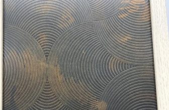
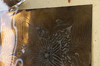
With the photoresist mask in place, the metal is submerged in an etchant solution, which selectively dissolves the exposed areas. The choice of etchant depends on the metal being processed. For instance, ferric chloride is commonly used for copper and stainless steel, while hydrofluoric acid may be employed for titanium, and alkaline solutions like sodium hydroxide are suitable for aluminum. The etching process can be isotropic, where material is removed uniformly in all directions, or anisotropic, where the etch rate varies with direction, depending on the etchant chemistry and metal crystal structure. For AI robot parts, isotropic etching is often preferred for creating smooth, rounded features, such as in fluidic channels, while anisotropic etching is used for sharper, vertical profiles, such as in microelectromechanical systems (MEMS) components.
The etching rate, typically measured in micrometers per minute, is a critical parameter that must be carefully controlled to achieve the desired depth and feature resolution. Factors influencing the etch rate include the concentration and temperature of the etchant, the agitation of the solution, and the metal’s grain structure. In industrial settings, these variables are optimized using statistical process control (SPC) techniques, ensuring repeatability and precision across large production runs. For AI robot parts, where components may range from macroscopic gears to nanoscale interconnects, etching depths can vary widely—from a few micrometers for thin-film circuits to several millimeters for structural elements—requiring tailored process conditions for each application.
Once etching is complete, the remaining photoresist is stripped away using a solvent or plasma ashing, revealing the final patterned metal. The etched part may undergo additional post-processing steps, such as polishing, passivation, or coating, to enhance its functionality. For example, a titanium robotic joint might be anodized to improve wear resistance, while a copper circuit trace might be plated with gold to enhance conductivity and prevent oxidation. These finishing steps are particularly important for AI robots operating in harsh environments, such as deep-sea exploration bots or planetary rovers, where component reliability is paramount.
One of the primary advantages of metal etching for AI robot parts is its ability to produce complex geometries without the mechanical stresses associated with traditional machining methods like milling or stamping. Unlike subtractive processes that rely on cutting tools, etching does not introduce burrs, microcracks, or heat-affected zones, preserving the integrity of the metal’s microstructure. This is especially beneficial for delicate components, such as the cantilever beams in MEMS accelerometers or the thin diaphragms in pressure sensors, where even minor defects could compromise performance. Furthermore, etching allows for batch processing, where multiple parts can be fabricated simultaneously on a single metal sheet, reducing production costs and time—a key consideration in the scalable manufacturing of AI robots.
The versatility of metal etching extends to its compatibility with a wide range of feature sizes, from macroscopic to microscopic scales. For AI robots, this scalability is invaluable. Consider the fabrication of a robotic gripper: the baseplate might require large, etched slots for mounting, while the fingertip sensors demand intricate, sub-millimeter patterns for tactile feedback. Chemical etching can accommodate both requirements in a single process, streamlining production and ensuring uniformity across components. Similarly, in the realm of microelectronics, etching is used to create the interconnects and vias in printed circuit boards (PCBs) that power AI algorithms, enabling seamless integration of hardware and software.
Beyond chemical etching, other variants of the process have found applications in AI robotics. Electrochemical etching, for instance, uses an electric current to enhance the removal of material, offering greater control over etch depth and sidewall profiles. This technique is particularly useful for creating high-aspect-ratio structures, such as the deep trenches in silicon-based MEMS devices adapted for robotic navigation systems. Laser etching, another alternative, employs a focused beam of light to ablate metal, providing exceptional precision for ultra-fine features. While laser etching is typically slower and more expensive than chemical methods, its non-contact nature makes it ideal for prototyping custom robot parts or etching heat-sensitive alloys.
The integration of metal etching into AI robot manufacturing has been driven by the growing complexity of robotic systems. Modern AI robots, such as those used in autonomous surgery, warehouse automation, or space exploration, rely on a synergy of mechanical, electrical, and computational elements. Etched metal parts play a pivotal role in each domain. In mechanical systems, they form the gears, linkages, and housings that enable precise movement. In electrical systems, they provide the conductive pathways and shielding that support high-speed data processing. In computational systems, they contribute to the miniaturization of sensors and actuators that execute AI-driven decisions in real time.
A notable example of metal etching in AI robotics is its use in producing components for soft robots—flexible, biomimetic machines that mimic the adaptability of living organisms. Soft robots often incorporate etched metal meshes or foils as reinforcement layers within elastomeric materials, providing structural support without sacrificing flexibility. For instance, a soft robotic actuator might feature an etched stainless steel lattice embedded in silicone, allowing it to bend and twist while maintaining durability. The precision of etching ensures that the lattice’s pore size and thickness are optimized for specific mechanical properties, such as tensile strength or elastic modulus, tailored to the robot’s intended task.
Another critical application lies in the fabrication of sensors, which serve as the sensory organs of AI robots. Etched metal components are integral to devices like capacitive pressure sensors, where thin, patterned diaphragms deform under force to detect changes in the environment, or resistive strain gauges, where etched grids measure deformation in robotic limbs. These sensors feed data into AI algorithms, enabling robots to perceive and respond to their surroundings with human-like acuity. The ability of etching to produce uniform, repeatable patterns ensures sensor reliability, a prerequisite for applications like robotic prosthetics or autonomous vehicles, where safety is non-negotiable.
The environmental impact of metal etching, while a concern in traditional manufacturing, has been mitigated in recent years through advancements in process efficiency and waste management. Early etching processes generated significant amounts of hazardous waste, such as spent etchants and metal-laden sludge, posing disposal challenges. However, modern facilities employ closed-loop systems that recycle etchants, reducing chemical consumption and minimizing environmental footprint. For AI robot production, where sustainability is increasingly prioritized, these innovations align with the industry’s shift toward green manufacturing practices. Additionally, the precision of etching reduces material waste compared to mechanical subtractive methods, as only the targeted areas of the metal are removed.
Looking ahead, the role of metal etching in AI robotics is poised to expand as new materials and techniques emerge. The advent of additive manufacturing, or 3D printing, has sparked interest in hybrid processes that combine etching with deposition methods, enabling the creation of multi-material components with unprecedented complexity. For example, a robotic actuator might integrate an etched titanium framework with a 3D-printed polymer coating, blending strength and flexibility in a single part. Similarly, advances in nanotechnology have opened the door to nanoetching, where features are defined at the atomic scale using techniques like reactive ion etching (RIE). This could lead to the development of next-generation AI robot components, such as ultra-compact processors or sensors with molecular-level sensitivity.
The scientific principles underlying metal etching are rooted in chemistry, physics, and materials science, making it a multidisciplinary endeavor. The kinetics of the etching reaction, for instance, follow Arrhenius behavior, where the rate increases exponentially with temperature, governed by the equation k = A * e^(-Ea/RT), where k is the rate constant, A is the pre-exponential factor, Ea is the activation energy, R is the gas constant, and T is the absolute temperature. This relationship allows engineers to fine-tune process conditions for optimal outcomes. Similarly, the diffusion of etchant molecules to the metal surface, described by Fick’s laws, influences feature uniformity, while the crystallographic orientation of the metal affects etch anisotropy, as certain planes etch faster due to differences in atomic packing density.
In practice, the design of etched parts for AI robots leverages computational tools like finite element analysis (FEA) and computational fluid dynamics (CFD) to simulate performance before fabrication. For a robotic gear, FEA might predict stress concentrations at tooth roots, guiding adjustments to the etched profile, while CFD could optimize the shape of an etched microfluidic channel to minimize pressure drop. These simulations, paired with real-time process monitoring—using techniques like optical emission spectroscopy to track etchant composition—ensure that the final product meets exacting specifications.
The economic implications of metal etching in AI robotics are significant, as the technology bridges the gap between prototyping and mass production. While the initial setup costs for photomask design and equipment can be high, the ability to produce thousands of identical parts in a single batch offsets these expenses, making etching cost-effective for large-scale deployment. This scalability has fueled the proliferation of AI robots in industries ranging from healthcare, where etched components enable precise surgical tools, to agriculture, where they power autonomous drones for crop monitoring.
Challenges remain, however, in pushing the boundaries of metal etching for AI applications. One limitation is the resolution of photochemical etching, which is constrained by the wavelength of UV light and the diffraction limit of the photomask. For features below 1 micrometer, alternative methods like electron beam lithography or extreme ultraviolet (EUV) lithography may be required, though these are costlier and less widespread. Another challenge is the etching of exotic alloys, such as shape-memory materials like nitinol, which exhibit unique phase-transition properties but resist conventional etchants, necessitating specialized chemistries or plasma-based approaches.
Despite these hurdles, the synergy between metal etching and AI robotics continues to deepen, driven by the relentless pace of technological innovation. Collaborative research between materials scientists, roboticists, and AI engineers has yielded breakthroughs like self-healing etched circuits, where microchannels deliver repair agents to damaged areas, or adaptive microstructures that reconfigure under electrical stimuli. These developments hint at a future where etched metal parts not only support AI robots but actively enhance their intelligence and autonomy.
In conclusion, metal etching stands as a linchpin in the fabrication of AI robot parts, offering a blend of precision, versatility, and efficiency that few other processes can match. Its ability to shape metals at multiple scales, from macroscopic frameworks to nanoscale circuits, underpins the functionality of robots that increasingly define our world. As the field advances, metal etching will likely remain at the forefront of robotic innovation, adapting to new challenges and unlocking possibilities yet unimagined. Whether in the delicate sensors of a medical bot or the rugged chassis of a Martian rover, etched metal components embody the fusion of art, science, and engineering that propels AI robotics into the future.