Metal etching is a sophisticated manufacturing process widely employed in the production of electrical connectors, critical components that facilitate the transmission of electrical signals or power between devices. This subtractive technique involves the selective removal of metal from a substrate using chemical or physical means to create intricate patterns, features, or structures. In the context of electrical connectors, metal etching offers unparalleled precision, enabling the fabrication of complex geometries that meet the demanding requirements of modern electronics, aerospace, automotive, and telecommunications industries. The process is valued for its ability to produce high-quality, reliable components with tight tolerances, excellent conductivity, and durability under harsh operating conditions.
Electrical connectors serve as the backbone of electrical systems, ensuring seamless connectivity in applications ranging from consumer electronics to industrial machinery. The choice of manufacturing technique significantly impacts the performance, cost, and scalability of these connectors. Metal etching stands out as a versatile method, capable of working with a variety of metals such as copper, stainless steel, nickel, and brass, which are commonly used in connector production due to their electrical and mechanical properties. This article explores the science, techniques, materials, and applications of metal etching for electrical connectors, delving into its advantages, limitations, and future prospects.
Historical Context of Metal Etching in Manufacturing
The origins of metal etching can be traced back centuries to artisanal practices, where acids were used to engrave decorative patterns onto armor and jewelry. However, its industrial application emerged in the 20th century with the advent of printed circuit board (PCB) manufacturing, where chemical etching became a cornerstone process. The adaptation of etching techniques for electrical connectors evolved alongside advancements in microelectronics and the growing demand for miniaturized, high-performance components.
By the mid-20th century, photochemical etching—also known as photoetching or chemical milling—gained prominence as a precise and repeatable method for producing intricate metal parts. This technique leveraged photographic processes to define patterns on metal surfaces, followed by chemical dissolution of unwanted material. The development of etching technology paralleled the rise of the electronics industry, where connectors needed to accommodate increasingly dense pin configurations and smaller form factors. Today, metal etching encompasses a range of methods, including wet chemical etching, dry etching (e.g., plasma etching), and laser-assisted etching, each tailored to specific connector designs and performance criteria.
Principles of Metal Etching
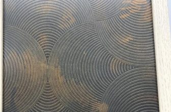
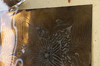
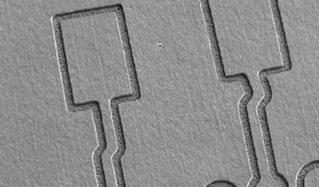
At its core, metal etching is a subtractive process that removes material from a metal workpiece to achieve a desired shape or pattern. The process begins with a metal substrate, typically in sheet or foil form, which is coated with a protective layer called a resist. The resist is selectively patterned to expose areas of the metal to an etchant—a chemical or physical agent that erodes the unprotected regions. The result is a precisely defined structure that retains the mechanical and electrical properties of the base metal.
The efficiency and outcome of etching depend on several factors, including the type of metal, the etchant used, the resist material, and the etching method. For electrical connectors, the goal is to create features such as contact pins, sockets, or shielding components with high dimensional accuracy and surface quality. Etching offers a distinct advantage over traditional mechanical methods like stamping or machining, as it avoids introducing mechanical stress or burrs that could compromise connector performance.
Types of Metal Etching Techniques
Wet Chemical Etching
Wet chemical etching is the most widely used technique for producing electrical connectors due to its cost-effectiveness and scalability. In this method, the metal substrate is immersed in or sprayed with a liquid etchant, typically an acid or alkaline solution, that dissolves the exposed metal. Common etchants include ferric chloride for copper, nitric acid for stainless steel, and cupric chloride for various alloys.
The process begins with the application of a photoresist—a light-sensitive polymer—onto the metal surface. A photomask, containing the connector design, is placed over the resist and exposed to ultraviolet (UV) light, hardening the resist in the desired pattern. The unexposed resist is then washed away, leaving the metal vulnerable to the etchant. After etching, the remaining resist is stripped, revealing the finished component.
Wet etching is isotropic, meaning it etches uniformly in all directions, which can lead to undercutting beneath the resist. While this limits the resolution for very fine features, advancements in resist materials and etchant chemistry have minimized these effects, making wet etching suitable for a wide range of connector designs.
Dry Etching
Dry etching, including plasma etching and reactive ion etching (RIE), uses gaseous etchants rather than liquids, offering greater control and anisotropy (directional etching). In plasma etching, a plasma—a partially ionized gas—is generated in a vacuum chamber, and reactive species bombard the metal surface to remove material. RIE enhances this process by applying an electric field to direct ions toward the substrate, achieving sharper edges and finer features.
Dry etching is particularly advantageous for high-precision connectors used in microelectronics, where feature sizes may be on the order of micrometers. However, its higher equipment costs and slower throughput compared to wet etching make it less common for large-scale connector production.
Laser Etching
Laser etching employs focused laser beams to ablate or vaporize metal from the substrate. This method offers exceptional precision and flexibility, as the laser can be programmed to follow complex patterns without the need for masks or resists. For electrical connectors, laser etching is often used to create microscale features or to refine components produced by other methods.
While laser etching excels in prototyping and small-batch production, its slower processing speed and higher operational costs limit its use in mass manufacturing. Nonetheless, it remains a valuable tool for custom or high-value connectors.
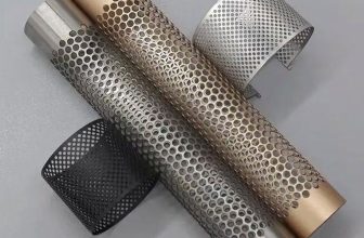
Materials Used in Metal Etching for Electrical Connectors
The choice of metal for electrical connectors is dictated by electrical conductivity, corrosion resistance, mechanical strength, and compatibility with etching processes. Below is an overview of commonly etched metals and their properties.
Copper
Copper is the most prevalent material for electrical connectors due to its excellent electrical conductivity (approximately 5.96 × 10^7 S/m at 20°C) and ductility. It is easily etched using ferric chloride or cupric chloride, making it ideal for wet chemical processes. Copper connectors are often plated with gold or nickel to enhance corrosion resistance and solderability.
Stainless Steel
Stainless steel, an iron-based alloy with chromium and nickel, offers superior corrosion resistance and mechanical strength. It is etched using nitric acid or hydrochloric acid-based solutions and is commonly used in connectors for harsh environments, such as aerospace or marine applications.
Nickel and Nickel Alloys
Nickel and its alloys, such as nickel silver (a copper-nickel-zinc alloy), provide a balance of conductivity, durability, and resistance to oxidation. These materials are etched with acidic solutions and are often employed in connectors requiring high wear resistance, such as those in automotive systems.
Brass
Brass, a copper-zinc alloy, combines good conductivity with machinability and corrosion resistance. It is etched similarly to copper and is frequently used in low-cost connectors for consumer electronics.
| Material | Electrical Conductivity (S/m) | Corrosion Resistance | Mechanical Strength | Common Etchant | Typical Applications |
|---|---|---|---|---|---|
| Copper | 5.96 × 10^7 | Moderate | Moderate | Ferric Chloride | General-purpose connectors |
| Stainless Steel | 1.45 × 10^6 | High | High | Nitric Acid | Harsh environment connectors |
| Nickel | 1.43 × 10^7 | High | High | Hydrochloric Acid | Wear-resistant connectors |
| Brass | 1.59 × 10^7 | Moderate | Moderate | Ferric Chloride | Consumer electronics |
Design Considerations in Metal Etching
Designing electrical connectors for etching requires careful consideration of feature size, tolerances, and material properties. The isotropic nature of wet etching, for instance, imposes limits on the minimum feature width—typically twice the metal thickness to avoid excessive undercutting. Dry etching and laser etching, with their anisotropic capabilities, allow for finer features but at a higher cost.
Connector designs must also account for electrical performance. For high-frequency applications, such as RF connectors, the etched surfaces must be smooth to minimize signal loss. Plating layers, such as gold or silver, are often added post-etching to enhance conductivity and reduce contact resistance.
Advantages of Metal Etching for Electrical Connectors
Metal etching offers several advantages over alternative manufacturing methods like stamping, machining, or additive processes:
- Precision and Complexity: Etching can produce intricate patterns and fine features without mechanical distortion, ideal for miniaturized connectors.
- Cost-Effectiveness: For medium to large production runs, wet etching is economical due to its scalability and minimal tooling requirements.
- Material Versatility: A wide range of metals and alloys can be etched, allowing customization for specific applications.
- Stress-Free Process: Unlike stamping, etching does not introduce residual stresses or burrs, ensuring the integrity of delicate connector components.
- Rapid Prototyping: Laser etching and photochemical processes enable quick iterations during the design phase.
Limitations of Metal Etching
Despite its strengths, metal etching has limitations that must be addressed:
- Resolution Constraints: Wet etching’s isotropic nature limits its ability to produce ultra-fine features compared to dry or laser methods.
- Environmental Concerns: Chemical etchants generate hazardous waste, requiring careful disposal and regulatory compliance.
- Thickness Limitations: Etching is most effective for thin metal sheets (typically <1.5 mm), making it less suitable for thick, robust connectors.
- Surface Finish: Etched surfaces may require additional polishing or plating to meet stringent smoothness requirements.
Applications of Etched Electrical Connectors
Etched electrical connectors find applications across diverse industries:
Consumer Electronics
In smartphones, laptops, and wearable devices, etched copper connectors provide reliable interconnects within compact assemblies. Their lightweight and precise construction support the trend toward miniaturization.
Automotive Industry
Etched stainless steel and nickel connectors are used in automotive wiring harnesses and sensors, where durability and resistance to heat and vibration are paramount.
Aerospace and Defense
High-performance connectors in aircraft and military equipment, often made from stainless steel or nickel alloys, rely on etching for precision and reliability under extreme conditions.
Telecommunications
RF and high-speed data connectors, etched from copper or brass, ensure low signal loss and high bandwidth in 5G infrastructure and satellite systems.
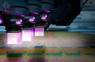
Process Optimization and Quality Control
Optimizing the etching process involves balancing etch rate, uniformity, and feature fidelity. Key parameters include etchant concentration, temperature, and exposure time. For example, in wet etching, a higher etchant concentration increases the etch rate but may reduce selectivity, risking damage to the resist.
Quality control is critical to ensure connector performance. Techniques such as optical microscopy, scanning electron microscopy (SEM), and profilometry are used to inspect feature dimensions, surface roughness, and edge quality. Electrical testing verifies conductivity and contact resistance, while environmental testing assesses corrosion resistance and durability.
| Parameter | Typical Range | Effect on Etching Process |
|---|---|---|
| Etchant Concentration | 10–40% | Higher concentration increases etch rate |
| Temperature | 20–60°C | Higher temperature accelerates etching |
| Exposure Time | 1–30 minutes | Longer time increases material removal |
| Resist Thickness | 5–50 μm | Thicker resist improves protection |
Conclusion
The future of metal etching is shaped by advancements in materials science, process technology, and industry demands. Emerging trends include:
- Nanoscale Etching: Techniques like atomic layer etching (ALE) promise sub-micrometer precision for next-generation connectors in quantum computing and nanotechnology.
- Sustainable Etching: Research into greener etchants, such as biodegradable chemicals or water-based solutions, aims to reduce environmental impact.
- Hybrid Processes: Combining etching with additive manufacturing (e.g., 3D printing) could enable the production of complex, multi-material connectors.
- Automation and AI: Machine learning algorithms are being integrated into etching systems to optimize parameters and predict outcomes, enhancing efficiency and quality.
Metal etching is a cornerstone technology in the production of electrical connectors, offering a unique blend of precision, versatility, and scalability. From wet chemical etching’s cost-effective simplicity to laser etching’s high-resolution capabilities, the process adapts to a wide range of materials and applications. As industries push toward smaller, more reliable, and environmentally sustainable components, metal etching continues to evolve, supported by innovations in chemistry, equipment, and design.
This article has provided a comprehensive overview of metal etching for electrical connectors, covering its principles, techniques, materials, and practical considerations. With its ability to meet the stringent demands of modern technology, metal etching remains a vital tool in the quest for connectivity in an increasingly electrified world.