Microlens arrays (MLAs) are essential components in various optical systems, including imaging devices, displays, and optical communications.
The fabrication of MLAs involves precise control over the shape, size, and surface quality of individual lenses. One of the critical techniques used in MLA fabrication is reactive ion beam etching (RIBE), which offers high precision and control over the etching process. This article delves into the research on the transfer of microlens array reactive ion beam etching, providing a comprehensive overview of the technology, its applications, and the latest advancements in the field.
Overview of Reactive Ion Beam Etching
Reactive ion beam etching is a dry etching process that utilizes a beam of reactive ions to selectively remove material from a substrate. The process involves the generation of a plasma, which contains reactive ions that are accelerated towards the substrate. The interaction between the reactive ions and the substrate material results in the removal of material through chemical reactions and physical sputtering.
RIBE offers several advantages over other etching techniques, including:
- High Anisotropy: The directional nature of the ion beam allows for precise control over the etching direction, resulting in highly anisotropic etching profiles.
- Selectivity: The chemical nature of the etching process allows for selective removal of specific materials, minimizing damage to underlying layers.
- Uniformity: The uniform distribution of the ion beam ensures consistent etching across the substrate, which is crucial for the fabrication of large-area MLAs.
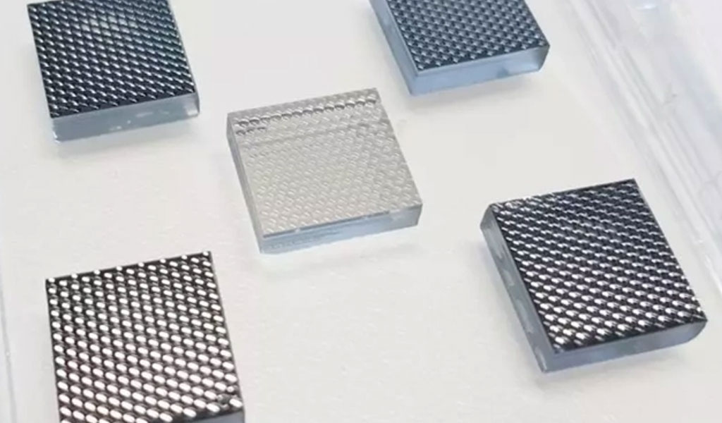
Microlens Array Fabrication Using RIBE
The fabrication of MLAs using RIBE involves several key steps:
- Substrate Preparation: The substrate material, typically a transparent material such as glass or polymer, is cleaned and prepared for the etching process.
- Mask Patterning: A mask is patterned on the substrate to define the areas to be etched. This can be achieved using photolithography or other patterning techniques.
- Etching Process: The substrate is exposed to the reactive ion beam, which selectively removes material from the unmasked areas. The etching parameters, such as ion beam energy, gas composition, and etching time, are carefully controlled to achieve the desired lens profile.
- Post-Processing: After etching, the substrate may undergo additional processing steps, such as cleaning and annealing, to improve the surface quality and optical properties of the MLAs.
Research on the Transfer of Microlens Array RIBE
The transfer of microlens array RIBE technology from research laboratories to industrial applications has been a focus of extensive research. Key areas of investigation include:
- Process Optimization: Researchers have explored various process parameters to optimize the etching profile and surface quality of MLAs. Table 1 summarizes some of the key parameters and their effects on the etching process.Table 1: Key Parameters in RIBE for MLA FabricationParameterEffect on Etching ProcessIon Beam EnergyInfluences etching rate and surface roughnessGas CompositionAffects selectivity and etching chemistryEtching TimeDetermines the depth and profile of the lensesChamber PressureImpacts plasma density and ion beam uniformitySubstrate TemperatureInfluences etching rate and surface quality
- Material Selection: The choice of substrate material plays a crucial role in the fabrication of MLAs. Research has focused on the etching characteristics of various materials, including glasses, polymers, and semiconductors. Table 2 provides a comparison of different substrate materials and their suitability for MLA fabrication using RIBE.Table 2: Comparison of Substrate Materials for MLA FabricationMaterialEtching RateSurface RoughnessOptical PropertiesSuitability for MLA FabricationFused SilicaHighLowExcellentHighBorosilicate GlassModerateModerateGoodModeratePolycarbonateLowHighFairLowSiliconHighLowGoodHigh
- Mask Patterning Techniques: The precision of the mask patterning process is critical for the fabrication of high-quality MLAs. Research has explored various patterning techniques, including photolithography, electron beam lithography, and nanoimprint lithography. Table 3 compares these techniques in terms of resolution, throughput, and cost.Table 3: Comparison of Mask Patterning TechniquesTechniqueResolutionThroughputCostSuitability for MLA FabricationPhotolithographyModerateHighLowHighElectron Beam LithographyHighLowHighModerateNanoimprint LithographyHighModerateModerateHigh
- Post-Processing Techniques: Post-processing steps, such as cleaning and annealing, are essential for improving the surface quality and optical properties of MLAs. Research has focused on optimizing these steps to achieve the desired optical performance. Table 4 summarizes some of the post-processing techniques and their effects on MLA properties.Table 4: Post-Processing Techniques for MLA FabricationTechniqueEffect on Surface QualityEffect on Optical PropertiesSuitability for MLA FabricationWet CleaningModerate improvementModerate improvementHighDry CleaningHigh improvementHigh improvementHighAnnealingHigh improvementHigh improvementHighChemical PolishingModerate improvementModerate improvementModerate
Applications of Microlens Arrays
MLAs fabricated using RIBE have a wide range of applications in various fields, including:
- Imaging Devices: MLAs are used in cameras, microscopes, and other imaging devices to enhance image quality and resolution. The precise control over the lens profile and surface quality offered by RIBE makes it an ideal technique for fabricating high-performance imaging MLAs.
- Displays: MLAs are used in displays, such as liquid crystal displays (LCDs) and organic light-emitting diode (OLED) displays, to improve brightness and viewing angles. The uniformity and precision of RIBE-fabricated MLAs ensure consistent optical performance across the display.
- Optical Communications: MLAs are used in optical communication systems to focus and collimate light beams, improving signal transmission and reducing losses. The high anisotropy and selectivity of RIBE allow for the fabrication of MLAs with precise optical properties, enhancing the performance of optical communication systems.
- Solar Concentrators: MLAs are used in solar concentrators to focus sunlight onto photovoltaic cells, increasing their efficiency. The ability of RIBE to fabricate large-area MLAs with uniform optical properties makes it a suitable technique for solar concentrator applications.
Challenges and Future Directions
Despite the advances in MLA fabrication using RIBE, several challenges remain. These include:
- Scalability: The transfer of RIBE technology from research laboratories to industrial-scale production requires addressing issues related to scalability, throughput, and cost-effectiveness.
- Material Compatibility: The etching characteristics of different materials need to be further investigated to expand the range of substrates suitable for MLA fabrication using RIBE.
- Process Control: The precise control over the etching process parameters is crucial for achieving the desired lens profile and surface quality. Further research is needed to optimize these parameters and develop robust process control strategies.
- Environmental Impact: The environmental impact of the etching process, including the generation and disposal of hazardous byproducts, needs to be addressed to ensure sustainable and eco-friendly MLA fabrication.
Future research directions in the field of MLA fabrication using RIBE include:
- Advanced Materials: Exploring new materials with unique optical properties and etching characteristics to enhance the performance of MLAs.
- Nanoscale Fabrication: Developing techniques for the fabrication of nanoscale MLAs with ultra-high resolution and precision.
- Integrated Systems: Integrating MLAs with other optical components, such as waveguides and detectors, to create compact and high-performance optical systems.
- Machine Learning: Applying machine learning algorithms to optimize the etching process parameters and improve the precision and efficiency of MLA fabrication.
Conclusion
The transfer of microlens array reactive ion beam etching from research to industrial applications represents a significant advancement in the field of optical technology. The precise control over the etching process, coupled with the ability to fabricate high-quality MLAs with uniform optical properties, makes RIBE a valuable technique for various applications. Continued research and development in this area will address the remaining challenges and pave the way for future innovations in MLA fabrication and optical technology.