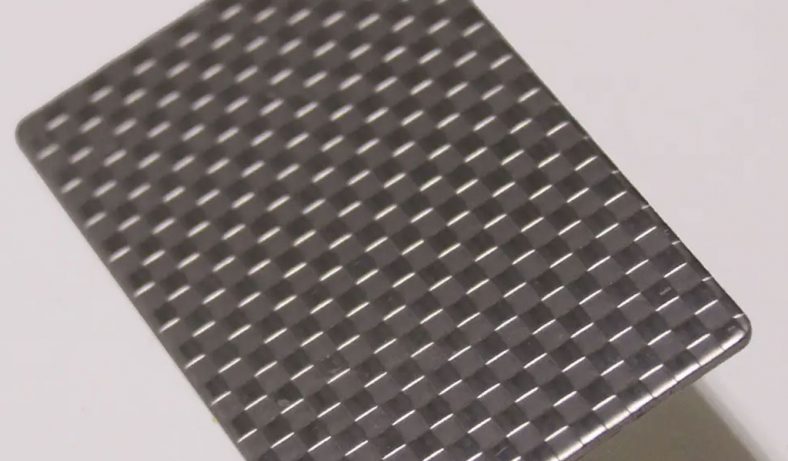
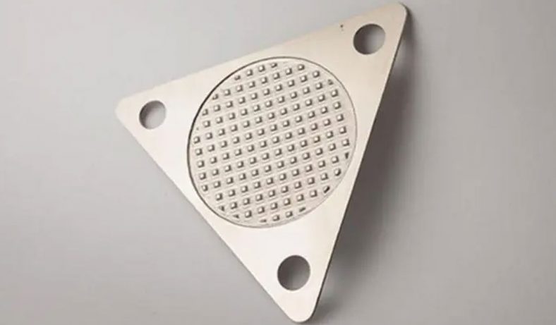
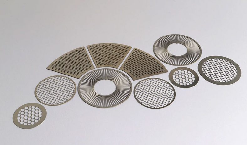
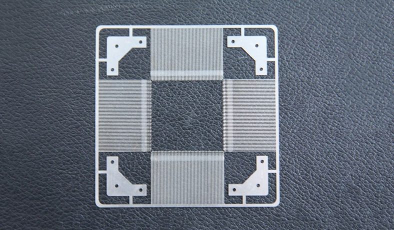
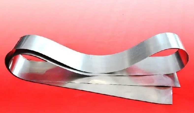
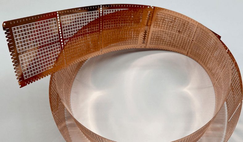
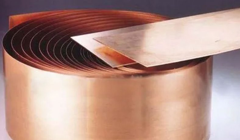
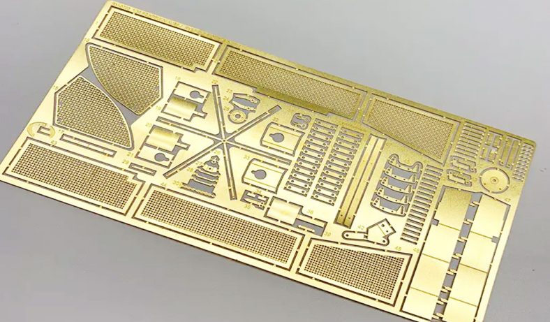
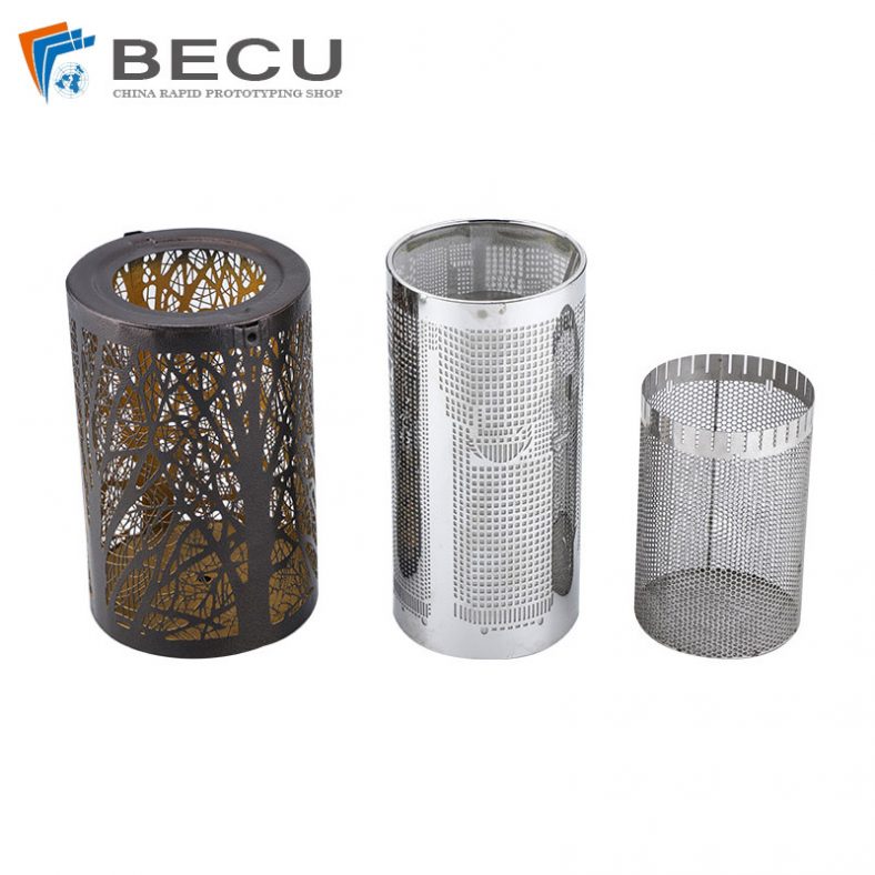
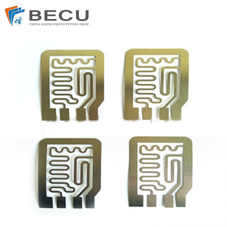
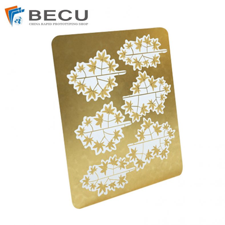
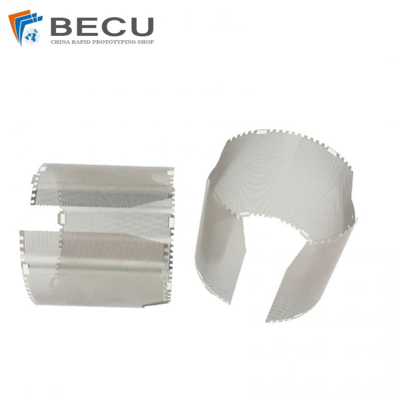
Metal etching is a critical process in microfabrication, semiconductor manufacturing, and materials science, where precise removal of material from a substrate is required to create intricate patterns, structures, or functional components. The etching rate, defined as the rate at which material is removed from the substrate surface (typically measured in units such as Å/min, nm/min, or μm/min), is a fundamental parameter that governs the quality, precision, and efficiency of the etching process. Achieving consistent and controlled etching rates is essential for ensuring the reproducibility of etched features, minimizing defects, and optimizing production throughput. However, variations in process conditions, such as temperature, gas composition, plasma power, or etchant concentration, can lead to fluctuations in etching rates, potentially compromising the integrity of the fabricated structures.
To address these challenges, online monitoring technology has emerged as a transformative approach to real-time measurement and control of etching rates during metal etching processes. Unlike traditional offline methods, which involve post-process measurements and may introduce delays or require additional sample preparation, online monitoring enables continuous, in-situ assessment of etching parameters. This capability is particularly valuable in high-precision applications, such as the fabrication of integrated circuits (ICs), microelectromechanical systems (MEMS), and advanced photonic devices, where even minor deviations in etching rate can result in significant performance degradation.
This article provides a comprehensive overview of online monitoring technology for etching rate in metal etching, covering its principles, methodologies, instrumentation, applications, and recent advancements. It explores the various techniques used for real-time etch rate monitoring, compares their strengths and limitations, and discusses their integration into modern etching systems. Detailed tables are included to facilitate comparison of monitoring technologies, and the article addresses emerging trends, challenges, and future directions in this rapidly evolving field.
Principles of Metal Etching and Etching Rate
Overview of Metal Etching
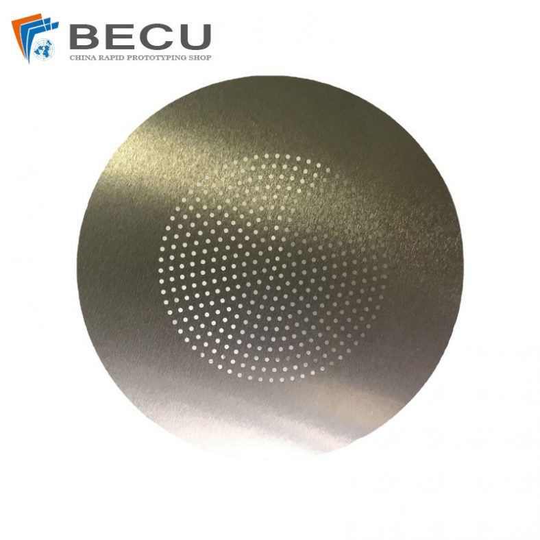
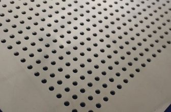
Metal etching is a subtractive manufacturing process used to selectively remove material from a metal substrate to create desired patterns or structures. It is widely employed in industries such as electronics, aerospace, and medical device manufacturing. The process can be broadly classified into two categories: wet etching and dry etching.
- Wet Etching: This involves immersing the substrate in a liquid chemical etchant, such as acids (e.g., nitric acid, hydrochloric acid) or bases, which react with the metal to dissolve the exposed material. Wet etching is typically isotropic, meaning it etches uniformly in all directions, which can lead to undercutting beneath the mask and limit feature resolution.
- Dry Etching: This uses gaseous etchants, often in a plasma environment, to remove material through chemical reactions, physical sputtering, or a combination of both. Dry etching techniques, such as reactive ion etching (RIE) and inductively coupled plasma (ICP) etching, offer greater anisotropy, enabling the creation of high-aspect-ratio features with vertical sidewalls.
Common metals etched in industrial applications include aluminum (Al), copper (Cu), titanium (Ti), nickel (Ni), and noble metals like gold (Au) and platinum (Pt). Each metal requires specific etchants and process conditions to achieve optimal results, as their chemical reactivity and volatility of reaction byproducts vary significantly.
Etching Rate: Definition and Importance
The etching rate is defined as the thickness of material removed per unit time, typically expressed in units such as angstroms per second (Å/s), nanometers per minute (nm/min), or micrometers per minute (μm/min). It is influenced by multiple factors, including:
- Process Parameters: Plasma power, gas flow rates, chamber pressure, and substrate temperature in dry etching; etchant concentration, temperature, and agitation in wet etching.
- Material Properties: The chemical composition, crystal structure, and surface morphology of the metal substrate.
- Mask Characteristics: The selectivity of the mask material (e.g., photoresist, silicon dioxide, or metal hard masks) relative to the substrate, which affects the etching profile and rate.
The etching rate directly impacts the dimensional accuracy, surface quality, and throughput of the etching process. For shallow etches, a slower etching rate may be preferred to maintain control, while deep etches often require higher rates to minimize processing time. However, uncontrolled variations in etching rate can lead to issues such as over-etching, under-etching, or non-uniform feature sizes, necessitating precise monitoring and control.
Challenges in Etching Rate Control
Achieving a consistent etching rate is challenging due to the dynamic nature of etching processes. Key challenges include:
- Process Drift: Gradual changes in plasma chemistry, etchant depletion, or chamber wall conditions can alter the etching rate over time.
- Non-Uniformity: Spatial variations across the substrate, such as edge-to-center differences in plasma density, can result in non-uniform etching rates.
- Material Variability: Differences in substrate composition, doping, or surface preparation can affect etching behavior.
- Real-Time Measurement: Traditional methods, such as post-process thickness measurements using profilometry or ellipsometry, are not suitable for real-time control, as they require interrupting the process.
Online monitoring technologies address these challenges by providing real-time data on etching rates, enabling process adjustments to maintain optimal conditions.
Online Monitoring Technologies for Etching Rate
Online monitoring of etching rates involves the use of in-situ sensors, optical diagnostics, and advanced data processing techniques to measure material removal rates during the etching process. These technologies can be broadly categorized into optical, electrical, and physical methods, each with distinct principles and applications.
Optical Monitoring Techniques
Optical techniques are among the most widely used for online etching rate monitoring due to their non-invasive nature and high sensitivity. They rely on the interaction of light with the substrate surface or plasma environment to infer etching characteristics.
Laser Interferometry
Principle: Laser interferometry measures changes in the thickness of a thin film or substrate by analyzing the interference patterns of laser light reflected from the surface. As material is etched, the film thickness decreases, altering the phase of the reflected light and producing oscillatory interference signals. The etching rate is calculated from the period of these oscillations, which is related to the wavelength of the laser and the refractive index of the material.
Implementation: A monochromatic laser (e.g., He-Ne laser at 632.8 nm) is directed at the substrate through a viewport in the etching chamber. The reflected light is collected by a photodetector, and the interference signal is processed to determine the etching rate. Dual-wavelength interferometry can be used to improve accuracy for multilayer films.
Advantages:
- High precision (sub-nanometer resolution).
- Suitable for both transparent and opaque films.
- Non-invasive and compatible with vacuum environments.
Limitations:
- Requires a smooth, reflective surface for accurate measurements.
- Signal interpretation can be complex for multilayer stacks or rough surfaces.
- Limited to line-of-sight measurements, which may not capture spatial variations.
Applications: Laser interferometry is widely used in plasma etching of silicon, silicon dioxide, and metal films, particularly in semiconductor manufacturing. It is effective for monitoring shallow etches where precise control is critical.
Reflectometry
Principle: Reflectometry measures the intensity of light reflected from the substrate surface, which changes as the film thickness is reduced during etching. Unlike interferometry, reflectometry does not rely on interference patterns but on the absolute reflectivity, which is influenced by the film’s optical properties and thickness.
Implementation: A broadband light source (e.g., xenon lamp) illuminates the substrate, and the reflected light is analyzed using a spectrometer. The reflectivity spectrum is compared to theoretical models to estimate the etching rate. In-situ reflectometry systems often use fiber-optic probes for integration into etching chambers.
Advantages:
- Broad applicability to various materials, including metals and dielectrics.
- Simpler signal interpretation compared to interferometry for some applications.
- Can measure multiple film properties (e.g., thickness, refractive index) simultaneously.
Limitations:
- Lower resolution compared to interferometry for very thin films.
- Sensitivity to surface roughness and optical absorption.
- Requires calibration for accurate quantitative measurements.
Applications: Reflectometry is used in both wet and dry etching processes, particularly for monitoring metal films like aluminum and copper in IC fabrication.
Optical Emission Spectroscopy (OES)
Principle: OES monitors the light emitted by excited species in the plasma during dry etching. The intensity of specific emission lines, corresponding to etch byproducts or reactants, correlates with the etching rate. For example, in metal etching, emission lines from metal halides (e.g., AlCl in aluminum etching) can indicate the rate of material removal.
Implementation: A spectrometer collects light from the plasma through a quartz window in the etching chamber. The emission spectra are analyzed to identify peaks associated with etch products, and their intensities are correlated with etching rates using calibration models. Advanced OES systems use machine learning to improve accuracy.
Advantages:
- Non-invasive and does not require direct substrate access.
- Provides information on plasma chemistry and process stability.
- Can monitor multiple species simultaneously.
Limitations:
- Indirect measurement, requiring calibration to relate emission intensity to etching rate.
- Sensitivity to plasma conditions, which may introduce noise.
- Limited to plasma-based etching processes.
Applications: OES is extensively used in RIE and ICP etching of metals, such as titanium and nickel, in MEMS and semiconductor applications.
Electrical Monitoring Techniques
Electrical methods measure changes in the electrical properties of the substrate or plasma to infer etching rates. These techniques are particularly useful for conductive materials like metals.
Impedance Spectroscopy
Principle: Impedance spectroscopy measures the electrical impedance of the substrate or etching chamber, which changes as material is removed. In plasma etching, the impedance of the plasma-substrate system is influenced by the thickness and conductivity of the etched layer.
Implementation: Electrodes are integrated into the etching chamber to apply an alternating current (AC) signal and measure the resulting impedance. The impedance data are analyzed to estimate the etching rate, often in conjunction with equivalent circuit models.
Advantages:
- Sensitive to changes in conductive films, making it ideal for metal etching.
- Can be integrated into existing plasma etching systems.
- Provides real-time feedback for process control.
Limitations:
- Requires complex signal processing and calibration.
- Limited to conductive or semi-conductive substrates.
- May be affected by plasma instabilities or chamber conditions.
Applications: Impedance spectroscopy is used in plasma etching of metals like copper and aluminum, particularly in applications requiring high selectivity.
Bias Voltage Monitoring
Principle: In plasma etching, the DC bias voltage on the substrate electrode is influenced by the ion energy and etching rate. Changes in the bias voltage can be correlated with the etching rate, especially in RIE processes where ion bombardment plays a significant role.
Implementation: The bias voltage is measured using a voltage probe connected to the substrate holder. Variations in the voltage are analyzed in real-time to estimate the etching rate, often using empirical calibration curves.
Advantages:
- Simple to implement in existing RIE systems.
- Provides direct insight into ion-driven etching mechanisms.
- Cost-effective compared to optical methods.
Limitations:
- Indirect measurement, requiring calibration.
- Sensitivity to plasma power and gas composition.
- Less effective for chemical-dominated etching processes.
Applications: Bias voltage monitoring is used in RIE of metals like titanium and tungsten, where physical sputtering contributes significantly to the etching rate.
Physical Monitoring Techniques
Physical methods involve direct measurement of material removal through mechanical or mass-based techniques. These are less common in online monitoring due to their invasive nature but are valuable in specific applications.
Quartz Crystal Microbalance (QCM)
Principle: QCM measures the mass change of a quartz crystal oscillator as material is deposited or removed during etching. By coating the crystal with the same metal being etched, the etching rate can be inferred from the frequency shift of the oscillator.
Implementation: A QCM sensor is placed in the etching chamber, exposed to the same process conditions as the substrate. The frequency shift is monitored in real-time and converted to an etching rate using the Sauerbrey equation.
Advantages:
- High sensitivity to mass changes (nanogram resolution).
- Direct measurement of material removal.
- Applicable to both wet and dry etching.
Limitations:
- Requires a representative sample on the QCM sensor, which may not match the substrate exactly.
- Sensitive to temperature and pressure variations.
- Limited to small-area measurements.
Applications: QCM is used in research settings for monitoring etching rates of metals like gold and silver in plasma and wet etching processes.
In-Situ Profilometry
Principle: In-situ profilometry uses a stylus or laser-based probe to measure the surface topography of the substrate during etching, directly determining the depth of material removed.
Implementation: A miniaturized profilometer is integrated into the etching chamber, scanning the substrate surface periodically. The depth data are used to calculate the etching rate in real-time.
Advantages:
- Direct measurement of etch depth.
- High spatial resolution for non-uniformity analysis.
- Applicable to a wide range of materials.
Limitations:
- Invasive and may interfere with the etching process.
- Limited to low-pressure or wet etching environments.
- Complex integration into vacuum systems.
Applications: In-situ profilometry is used in specialized applications, such as wet etching of copper for printed circuit boards (PCBs).
Comparison of Online Monitoring Technologies
The following tables compare the key characteristics, advantages, and limitations of the primary online monitoring technologies for etching rate in metal etching. These tables provide a detailed reference for selecting the appropriate method based on application requirements.
Table 1: Comparison of Optical Monitoring Techniques
| Technique | Principle | Materials | Resolution | Advantages | Limitations | Applications |
|---|---|---|---|---|---|---|
| Laser Interferometry | Interference of reflected laser light to measure film thickness changes | Metals, dielectrics, semiconductors | Sub-nanometer | High precision, non-invasive, suitable for vacuum environments | Requires smooth surfaces, complex signal interpretation | Semiconductor IC fabrication, MEMS |
| Reflectometry | Measurement of reflected light intensity to estimate film thickness | Metals, dielectrics | Nanometer | Broad applicability, simpler signal processing, multi-property measurement | Lower resolution for thin films, sensitive to surface roughness | Metal etching in ICs, PCB manufacturing |
| Optical Emission Spectroscopy | Analysis of plasma emission lines to correlate with etch byproducts | Metals (plasma etching only) | Varies (indirect) | Non-invasive, monitors plasma chemistry, multi-species detection | Requires calibration, sensitive to plasma conditions | RIE, ICP etching of Ti, Ni, Al |
Table 2: Comparison of Electrical and Physical Monitoring Techniques
| Technique | Principle | Materials | Resolution | Advantages | Limitations | Applications |
|---|---|---|---|---|---|---|
| Impedance Spectroscopy | Measurement of electrical impedance changes during etching | Conductive metals | Varies (indirect) | Sensitive to conductive films, integrable into plasma systems | Complex signal processing, limited to conductive substrates | Cu, Al etching in ICs |
| Bias Voltage Monitoring | Correlation of DC bias voltage changes with etching rate | Metals (RIE processes) | Varies (indirect) | Simple implementation, cost-effective, insight into ion-driven etching | Indirect, sensitive to plasma conditions, less effective for chemical etching | RIE of Ti, W |
| Quartz Crystal Microbalance | Measurement of mass loss via frequency shift of a quartz oscillator | Metals, thin films | Nanogram | High sensitivity, direct measurement, applicable to wet/dry etching | Requires representative sample, sensitive to environmental variations | Research, Au, Ag etching |
| In-Situ Profilometry | Direct measurement of etch depth using a stylus or laser probe | Metals, dielectrics | Micrometer | Direct depth measurement, high spatial resolution | Invasive, complex integration, limited to specific environments | Wet etching of Cu for PCBs |
Integration into Etching Systems
System Design Considerations
Integrating online monitoring technologies into etching systems requires careful consideration of hardware compatibility, data acquisition, and process control. Key design considerations include:
- Chamber Compatibility: Monitoring equipment must withstand the harsh conditions of etching chambers, including vacuum, high temperatures, and corrosive gases. For example, optical viewports must be made of materials like quartz to resist plasma damage.
- Real-Time Data Processing: High-speed data acquisition systems are needed to process signals from sensors like interferometers or spectrometers. Machine learning algorithms can enhance data interpretation and enable predictive control.
- Feedback Control: Online monitoring systems are often coupled with feedback loops to adjust process parameters (e.g., gas flow, plasma power) in real-time, ensuring consistent etching rates. Advanced process control (APC) techniques are increasingly used for this purpose.
- Spatial Resolution: For large substrates, multiple sensors or scanning systems may be required to capture spatial variations in etching rate, addressing non-uniformity issues.
Case Studies
Semiconductor Manufacturing
In semiconductor fabrication, online monitoring is critical for etching metal interconnects (e.g., copper, aluminum) in advanced nodes (e.g., 5 nm, 3 nm). Laser interferometry and OES are commonly used to monitor etching rates during RIE processes. For example, a study demonstrated the use of OES to monitor aluminum etching in a chlorine-based plasma, achieving a precision of ±2 nm/min by correlating AlCl emission lines with etching rate.
MEMS Fabrication
In MEMS manufacturing, high-aspect-ratio etching of metals like titanium is required for creating microstructures. Bias voltage monitoring has been employed in ICP-RIE systems to control etching rates, ensuring uniform feature depths across 6-inch wafers. A reported implementation achieved a repeatability of ±1% by adjusting bias power based on real-time voltage data.
Wet Etching for PCBs
In wet etching of copper for PCBs, reflectometry has been integrated into spray etching systems to monitor etching rates in real-time. By measuring reflectivity changes, the system maintained an etching rate of 1 μm/min with a uniformity of ±5%, reducing defects in fine-line circuits.
Recent Advancements in Online Monitoring
Machine Learning and Artificial Intelligence
The integration of machine learning (ML) and artificial intelligence (AI) has revolutionized online monitoring of etching rates. ML models, such as artificial neural networks (ANNs) and Bayesian neural networks (BNNs), are used to analyze complex sensor data and predict etching rates with high accuracy. A recent study demonstrated the use of ANNs for in-situ etch depth prediction in plasma etching, achieving a prediction error of less than 1 nm by combining OES and digital image colorimetry data.
AI-driven systems also enable adaptive process control, where etching parameters are dynamically adjusted based on real-time predictions. For example, reinforcement learning algorithms have been applied to optimize gas flow rates in ICP-RIE, improving etching uniformity by 10% compared to traditional methods.
Non-Contact Monitoring
Non-contact techniques, such as digital image colorimetry and hyperspectral imaging, are gaining traction for monitoring etching rates in both wet and dry processes. These methods analyze color or spectral changes on the substrate surface to estimate material removal. A 2025 study reported the use of hyperspectral imaging to monitor copper etching in a wet process, achieving a resolution of 0.5 nm/min without physical contact.
Multi-Sensor Fusion
Combining multiple monitoring techniques (e.g., OES, interferometry, and bias voltage monitoring) enhances the robustness and accuracy of etching rate measurements. Multi-sensor fusion leverages complementary data to overcome the limitations of individual methods. For instance, a hybrid system integrating OES and QCM was used to monitor nickel etching in a plasma process, achieving a precision of ±0.5 nm/min by cross-validating emission and mass loss data.
Applications of Online Monitoring in Metal Etching
Semiconductor Industry
Online monitoring is indispensable in the semiconductor industry, where metal etching is used to form interconnects, vias, and electrodes. Real-time control of etching rates ensures the reliability of nanoscale features in advanced ICs. For example, copper damascene processes rely on OES to monitor etching rates during trench formation, maintaining critical dimension (CD) control within ±1 nm.
Semiconductor Industry
Online monitoring is indispensable in the semiconductor industry, where metal etching is used to form interconnects, vias, and electrodes. Real-time control of etchingOI rates ensures the reliability of nanoscale features in advanced ICs. For example, copper damascene processes rely on OES to monitor etching rates during trench formation, maintaining critical dimension (CD) control within ±1 nm.
MEMS and Nanotechnology
In MEMS and nanotechnology, online monitoring enables the fabrication of high-aspect-ratio metal structures with precise dimensions. Techniques like laser interferometry and bias voltage monitoring are used to achieve etching rates of 0.5–2 μm/min for materials like titanium and nickel, ensuring uniformity in complex 3D structures.
Aerospace and Medical Devices
In aerospace and medical device manufacturing, metal etching is used to create lightweight components and biocompatible surfaces. Reflectometry and QCM are employed to monitor etching rates for materials like titanium and stainless steel, ensuring surface quality and dimensional accuracy.
Challenges and Future Directions
Current Challenges
Despite significant advancements, online monitoring of etching rates faces several challenges:
- Calibration and Accuracy: Many techniques, such as OES and bias voltage monitoring, require precise calibration to achieve accurate etching rate measurements, which can be time-consuming and application-specific.
- Integration Complexity: Incorporating monitoring systems into existing etching equipment can be complex, requiring modifications to chamber design and control systems.
- Data Overload: The high volume of data generated by real-time monitoring systems necessitates robust data processing and storage solutions to avoid bottlenecks in process control.
- Cost: Advanced monitoring technologies, such as hyperspectral imaging and multi-sensor fusion systems, can be expensive, limiting their adoption in smaller-scale operations.
Emerging Trends
Several trends are shaping the future of online monitoring technology:
- AI and Machine Learning: The continued integration of AI and ML will enhance the predictive accuracy and automation of etching rate monitoring, enabling fully autonomous etching systems.
- Miniaturized Sensors: Advances in microfabrication are leading to smaller, more robust sensors that can be integrated directly into etching chambers, improving spatial resolution and reducing costs.
- Green Etching Processes: Online monitoring is being adapted to support environmentally friendly etching processes, such as those using alternative etchants with lower toxicity, by providing real-time feedback on process efficiency.
- Hybrid Monitoring Systems: The development of hybrid systems combining optical, electrical, and physical monitoring techniques will provide comprehensive data for optimizing etching processes across diverse applications.
Future Directions
The future of online monitoring technology lies in achieving greater integration, automation, and sustainability. Key areas of focus include:
- Standardization: Developing industry-wide standards for monitoring protocols and data formats to facilitate interoperability and reduce implementation barriers.
- Real-Time Predictive Maintenance: Using monitoring data to predict equipment wear and maintenance needs, minimizing downtime and extending the lifespan of etching systems.
- Scalability: Adapting monitoring technologies for large-scale manufacturing, such as roll-to-roll etching for flexible electronics, by improving sensor arrays and data processing capabilities.
- Cross-Disciplinary Applications: Expanding the use of online monitoring to emerging fields like quantum computing and biomedicine, where precise metal etching is critical for device performance.
Conclusion
Online monitoring technology for etching rate in metal etching represents a cornerstone of modern microfabrication, enabling unprecedented control over material removal processes in industries ranging from semiconductors to aerospace. By providing real-time data on etching rates, these technologies ensure the precision, uniformity, and efficiency required for advanced manufacturing. Optical techniques like laser interferometry and OES, electrical methods like impedance spectroscopy, and physical approaches like QCM offer complementary strengths, addressing diverse application needs. Recent advancements in AI, non-contact monitoring, and multi-sensor fusion are pushing the boundaries of what is possible, while challenges like calibration complexity and cost remain areas for improvement.
As the demand for smaller, more complex devices continues to grow, online monitoring will play an increasingly vital role in meeting these challenges. By integrating advanced sensors, predictive algorithms, and sustainable practices, the field is poised to drive innovation in metal etching, shaping the future of manufacturing and materials science. The detailed comparisons provided in this article underscore the diversity and potential of these technologies, offering a roadmap for researchers, engineers, and manufacturers to optimize etching processes for the next generation of technological advancements.

