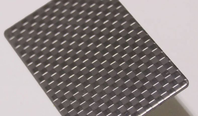
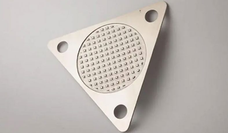
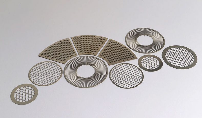
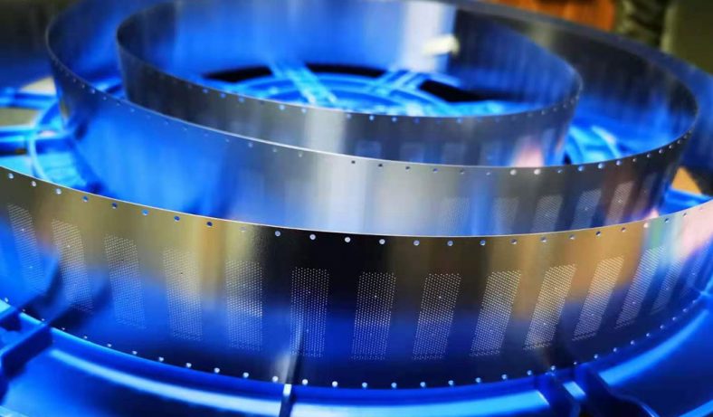
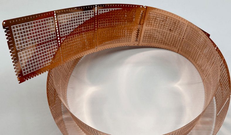
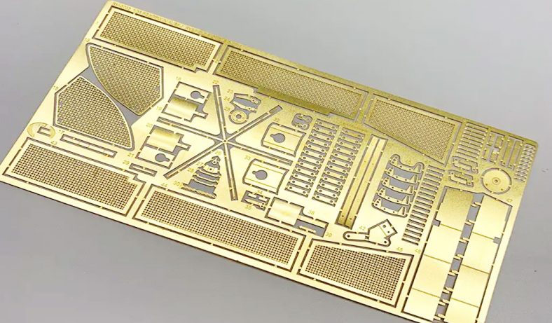
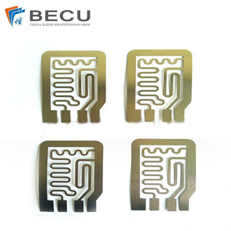
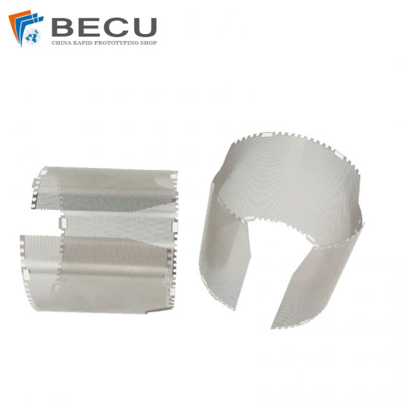
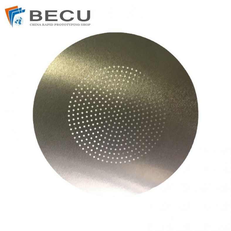
Resist stripping is a critical step in the metal etching process, particularly in microelectronics, printed circuit board (PCB) manufacturing, and precision metal fabrication. This process involves the removal of photoresist—a light-sensitive material used to define patterns during etching—from the substrate after the etching process is complete. The efficiency, precision, and environmental impact of resist stripping directly influence the quality of the final product, production throughput, and sustainability of manufacturing processes. Over the past few decades, significant research has been devoted to optimizing resist stripping technologies to meet the demands of shrinking feature sizes, complex material stacks, and stringent environmental regulations. This article provides a comprehensive exploration of the optimization research in resist stripping technology for metal etching, covering historical developments, fundamental principles, recent advancements, comparative analyses, and future directions.
1. Introduction to Resist Stripping in Metal Etching
1.1 Overview of Metal Etching
Metal etching is a subtractive manufacturing process used to selectively remove material from a metal substrate to create precise patterns, features, or components. It is widely employed in industries such as semiconductor manufacturing, PCB production, and microelectromechanical systems (MEMS). The process typically involves applying a photoresist layer to the metal surface, exposing it to light through a mask to define the desired pattern, developing the resist to expose specific areas, and then etching away the unprotected metal using chemical or physical means. After etching, the photoresist must be removed to reveal the final patterned metal surface, a step known as resist stripping.
1.2 Importance of Resist Stripping
Resist stripping is essential for ensuring the integrity of the etched metal features. Residual resist can lead to defects, such as incomplete circuit paths in PCBs or unreliable semiconductor devices. The stripping process must be thorough, selective (removing only the resist without damaging the underlying metal or substrate), and compatible with the materials used in the etching process. As feature sizes in microelectronics have scaled down to nanometer dimensions, the requirements for resist stripping have become more stringent, necessitating advancements in stripping technologies.
1.3 Challenges in Resist Stripping
The optimization of resist stripping faces several challenges:
- Material Compatibility: Stripping processes must avoid damaging sensitive metal layers (e.g., copper, aluminum, or titanium) or underlying substrates (e.g., silicon or glass).
- Resist Hardening: High-energy processes like plasma etching or ion implantation can harden the photoresist, making it difficult to remove.
- Environmental Concerns: Traditional wet stripping methods often use hazardous chemicals, raising concerns about waste disposal and worker safety.
- Process Efficiency: Stripping must be fast and cost-effective to maintain high production throughput, especially in high-volume manufacturing (HVM).
- Residue Control: Post-stripping residues can compromise device performance, requiring robust cleaning processes.
These challenges have driven extensive research into optimizing resist stripping techniques, with a focus on improving selectivity, reducing environmental impact, and enhancing process control.
2. Historical Context of Resist Stripping Technologies
2.1 Early Developments
The origins of resist stripping can be traced to the early days of photolithography in the mid-20th century, when wet chemical etching was the dominant method for patterning metal films. Early stripping processes relied on simple solvent-based solutions, such as acetone or alcohol, to dissolve organic photoresists. These methods were effective for the relatively large feature sizes (on the order of micrometers) and simple material stacks used in early integrated circuits (ICs) and PCBs.
2.2 Transition to Plasma-Based Stripping
By the 1970s, as IC complexity increased and feature sizes decreased, plasma-based dry stripping emerged as a viable alternative to wet stripping. Oxygen plasma, in particular, became widely adopted due to its ability to oxidize and volatilize organic photoresists, leaving minimal residues. The introduction of plasma stripping marked a significant shift, enabling better control over the stripping process and compatibility with more complex substrates.
2.3 Advancements in Wet Stripping
Despite the rise of dry stripping, wet stripping remained prevalent in industries like PCB manufacturing, where cost considerations and large substrate sizes favored liquid-based processes. In the 1980s and 1990s, new chemical formulations, such as alkaline strippers (e.g., sodium hydroxide or potassium hydroxide solutions) and proprietary solvent blends, were developed to address the challenges of hardened resists and improve stripping efficiency.
2.4 Environmental and Regulatory Pressures
The late 20th and early 21st centuries saw growing environmental concerns about the use of hazardous chemicals in wet stripping. Regulations such as the European Union’s Restriction of Hazardous Substances (RoHS) directive and the U.S. Environmental Protection Agency’s (EPA) guidelines prompted research into greener stripping chemistries and processes. This period also saw increased interest in dry stripping methods, such as supercritical carbon dioxide (CO₂) and laser-based stripping, as alternatives to traditional chemical methods.
3. Fundamental Principles of Resist Stripping
3.1 Photoresist Chemistry
Photoresists are typically organic polymers that undergo chemical changes upon exposure to light. Positive photoresists become soluble in a developer after exposure, while negative photoresists become insoluble. The chemical composition of the resist (e.g., novolac resins, poly(methyl methacrylate), or chemically amplified resists) determines its interaction with stripping agents. Understanding resist chemistry is crucial for designing effective stripping processes.
3.2 Wet Stripping Mechanisms
Wet stripping involves the use of liquid chemicals to dissolve or chemically react with the photoresist. Common wet stripping agents include:
- Solvents: Organic solvents like N-methyl-2-pyrrolidone (NMP) or dimethyl sulfoxide (DMSO) dissolve the resist by breaking intermolecular bonds.
- Alkaline Solutions: Sodium hydroxide (NaOH) or potassium hydroxide (KOH) solutions hydrolyze the resist, particularly effective for negative resists.
- Acidic Solutions: Sulfuric acid (H₂SO₄) combined with hydrogen peroxide (H₂O₂), known as piranha solution, oxidizes and removes organic resists.
- Proprietary Blends: Commercial strippers often combine solvents, surfactants, and chelating agents to enhance performance and selectivity.
The effectiveness of wet stripping depends on factors such as temperature, concentration, immersion time, and agitation.
3.3 Dry Stripping Mechanisms
Dry stripping uses gaseous or plasma-based processes to remove the resist. The most common dry stripping methods are:
- Oxygen Plasma Stripping: Oxygen plasma generates reactive oxygen species that oxidize the resist, converting it into volatile compounds like CO₂ and H₂O.
- Fluorine-Based Plasma: Fluorine-containing gases (e.g., CF₄ or SF₆) are used for resists that require additional chemical reactivity, often in combination with oxygen.
- UV/Ozone Stripping: Ultraviolet light in the presence of ozone breaks down the resist through photochemical reactions.
- Supercritical CO₂ Stripping: Supercritical CO₂, with or without co-solvents, dissolves the resist in a high-pressure, low-temperature environment.
Dry stripping offers advantages in terms of residue control and compatibility with delicate substrates but requires sophisticated equipment and precise process control.
3.4 Key Parameters in Resist Stripping
The optimization of resist stripping involves tuning several parameters:
- Selectivity: The stripping process must remove the resist without etching the underlying metal or substrate.
- Rate: Faster stripping rates improve throughput but may compromise selectivity or uniformity.
- Residue: Minimizing post-stripping residues is critical for device reliability.
- Uniformity: The stripping process must be consistent across the substrate, especially for large-area applications like PCBs.
- Environmental Impact: The choice of chemicals and waste management strategies affects the sustainability of the process.
4. Optimization Strategies in Resist Stripping
4.1 Process Parameter Optimization
Research into resist stripping optimization often focuses on fine-tuning process parameters. For wet stripping, key parameters include chemical concentration, temperature, and immersion time. For example, a study published by IEEE explored the optimization of a resist strip process on an Applied Materials Decoupled Plasma Source (DPS) 5200 metal etch platform, using a design of experiment (DOE) to evaluate strip time, passivation time, gas flow (e.g., CF₄), and temperature. The results showed that balancing strip time and gas flow was critical for minimizing residual resist while maintaining throughput.
In dry stripping, parameters such as plasma power, gas composition, and pressure are critical. For instance, oxygen plasma stripping requires careful control of radio frequency (RF) power to avoid substrate damage, while fluorine-based plasmas must balance etch rate and seletivity.
4.2 Advanced Chemical Formulations
The development of advanced stripping chemistries has been a major focus of optimization research. For wet stripping, proprietary formulations combining solvents, surfactants, and corrosion inhibitors have improved performance on hardened resists. For example, commercial strippers like EKC265 and ACT NE-14 are designed to remove resists after high-dose ion implantation, offering high selectivity to metals like aluminum and copper.
In dry stripping, the introduction of novel gas mixtures, such as H₂/N₂ plasmas, has enabled low-damage stripping for advanced nodes in semiconductor manufacturing. These mixtures reduce the risk of oxidation on metal surfaces compared to traditional O₂ plasmas.
4.3 Equipment Innovations
Advancements in stripping equipment have played a significant role in optimization. Modern wet stripping systems incorporate high-pressure spray nozzles, automated chemical delivery, and real-time monitoring to improve uniformity and reduce chemical consumption. Chemcut, a leading manufacturer of stripping equipment, emphasizes the importance of high-pressure options (100–500 psi) for removing resist after plating steps, which can trap resist under metal overhangs.
For dry stripping, tools like the Lam Research Kiyo series and Applied Materials Centura platforms offer precise control over plasma parameters, enabling tailored stripping processes for specific applications. These systems often integrate in-situ monitoring to detect endpoints and prevent over-stripping.
4.4 Environmental Optimization
Environmental considerations have driven research into greener stripping technologies. Wet stripping processes are being optimized to use biodegradable solvents and lower-toxicity chemicals. For example, replacing piranha solution with ozone-based aqueous chemistries reduces the environmental footprint of stripping.
Dry stripping methods, such as supercritical CO₂, eliminate the need for liquid chemicals entirely, offering a sustainable alternative. Research into supercritical CO₂ stripping has shown promise for removing resists from delicate substrates without generating hazardous waste, although challenges remain in scaling the technology for HVM.
4.5 Automation and Process Control
Automation and real-time process control are critical for optimizing resist stripping in high-throughput environments. Automated optical inspection (AOI) systems, as used in PCB manufacturing, scan substrates post-stripping to detect residual resist or defects, enabling immediate process adjustments. Machine learning algorithms are increasingly being applied to optimize stripping parameters dynamically, improving uniformity and yield. For example, a study on plasma etching optimization highlighted the potential of machine learning to adjust parameters in real-time, a concept that can be extended to resist stripping.
5. Comparative Analysis of Resist Stripping Technologies
To provide a detailed comparison of resist stripping technologies, the following tables summarize key attributes, performance metrics, and recent research findings.
5.1 Comparison of Wet vs. Dry Stripping Technologies
| Attribute | Wet Stripping | Dry Stripping |
|---|---|---|
| Mechanism | Chemical dissolution or reaction using liquid solvents, acids, or bases | Plasma, UV/ozone, or supercritical fluid-based removal |
| Common Chemistries | NMP, DMSO, NaOH, H₂SO₄/H₂O₂, proprietary blends | O₂, CF₄, H₂/N₂ plasmas, supercritical CO₂ |
| Equipment | Immersion tanks, spray systems, automated strippers | Plasma etchers, UV/ozone chambers, supercritical CO₂ systems |
| Selectivity | High with optimized chemistries; risk of metal corrosion | High with low-damage plasmas; risk of substrate damage at high power |
| Residue Control | Moderate; requires thorough rinsing | Excellent; minimal residues with proper endpoint detection |
| Environmental Impact | High; hazardous waste from solvents and acids | Lower; reduced chemical use, but energy-intensive for plasma systems |
| Cost | Low for simple setups; higher for proprietary chemistries | High due to equipment and energy costs |
| Applications | PCB manufacturing, chemical milling, large-area substrates | Semiconductor manufacturing, MEMS, advanced nodes |
| Recent Advancements | Biodegradable solvents, high-pressure spray systems | H₂/N₂ plasmas, supercritical CO₂, in-situ monitoring |
Table Notes: Wet stripping is preferred for cost-sensitive applications like PCB manufacturing, while dry stripping dominates in semiconductor fabrication due to its precision and residue control. Recent advancements in wet stripping focus on reducing environmental impact, while dry stripping research emphasizes low-damage processes for advanced nodes.
5.2 Performance Metrics of Common Stripping Chemistries
| Chemistry | Strip Rate (nm/min) | Selectivity to Cu/Al | Residue Level | Environmental Impact | Key Applications |
|---|---|---|---|---|---|
| NMP-Based Solvents | 100–500 | High | Moderate | High (toxic waste) | PCB, chemical milling |
| NaOH (Alkaline) | 200–1000 | Moderate (Cu corrosion) | High | Moderate | PCB, low-cost applications |
| H₂SO₄/H₂O₂ (Piranha) | 500–2000 | Low (metal attack) | Low | High (acid waste) | Semiconductor, post-implant stripping |
| O₂ Plasma | 50–300 | High | Very Low | Low | Semiconductor, MEMS |
| CF₄/O₂ Plasma | 100–500 | Moderate | Low | Moderate (fluorine emissions) | Advanced nodes, hardened resists |
| H₂/N₂ Plasma | 20–100 | Very High | Very Low | Low | 7 nm and below nodes |
| Supercritical CO₂ | 10–50 | Very High | Very Low | Very Low | Research, delicate substrates |
Table Notes: Strip rates vary depending on resist type and process conditions. H₂/N₂ plasmas and supercritical CO₂ offer superior selectivity and residue control but are slower and less mature. Piranha solution is fast but poses significant environmental and safety challenges.
5.3 Recent Research Findings (2015–2025)
| Study | Year | Technology | Key Findings | Source |
|---|---|---|---|---|
| IEEE Resist Strip DOE | 2015 | CF₄/O₂ Plasma | Optimized strip time and CF₄ flow reduced residual resist by 80% on BiCMOS wafers | |
| Chemcut High-Pressure Spray | 2020 | Wet Stripping | High-pressure (100–500 psi) spray improved resist removal after plating steps | |
| Stanford Nanofabrication | 2020 | Dry/Wet Hybrid | Hybrid process effective for hardened resists post-ion implantation | |
| Springer MACE Review | 2024 | Wet Stripping (HF-Based) | HF-based stripping optimized for nanostructure formation in semiconductors | |
| AIP Plasma Etching | 2024 | H₂/N₂ Plasma | Low-damage stripping achieved for 3 nm node semiconductor devices |
Table Notes: Recent studies highlight the trend toward low-damage, environmentally friendly stripping processes. Hybrid dry/wet approaches and advanced plasma chemistries are gaining traction for challenging applications.
6. Case Studies in Resist Stripping Optimization
6.1 Semiconductor Manufacturing: 3 nm Node
In semiconductor manufacturing, resist stripping for advanced nodes (e.g., 3 nm) requires extreme precision to avoid damaging ultra-thin metal layers. A 2024 study published by AIP Publishing demonstrated the use of H₂/N₂ plasma for resist stripping in 3 nm node devices. The low ion energy of H₂/N₂ plasma minimized damage to copper interconnects, achieving a strip rate of 50 nm/min with no detectable residues. The study also employed in-situ optical emission spectroscopy (OES) for endpoint detection, ensuring process repeatability.
6.2 PCB Manufacturing: High-Throughput Stripping
In PCB manufacturing, wet stripping remains dominant due to its cost-effectiveness. A 2024 article by TechSparks highlighted the optimization of alkaline stripping processes for high-throughput PCB production. By maintaining the pH of the stripping solution below 8.5 and using high-pressure spray nozzles, the process achieved a strip rate of 1000 nm/min with minimal copper corrosion. Automated optical inspection (AOI) was integrated to detect residual resist, reducing defect rates by 90%.
6.3 MEMS Fabrication: Hybrid Stripping
MEMS devices often involve complex material stacks, requiring tailored stripping processes. A 2021 study by the Stanford Nanofabrication Facility explored a hybrid dry/wet stripping process for MEMS wafers with hardened resists post-plasma etching. The process combined oxygen plasma stripping to remove the bulk resist, followed by a dilute NaOH rinse to eliminate residues. This approach achieved high selectivity to silicon and metal layers, with a residue level below 0.1% as confirmed by scanning electron microscopy (SEM).
7. Environmental and Sustainability Considerations
7.1 Hazardous Waste Reduction
Traditional wet stripping processes generate significant hazardous waste, including spent solvents and acidic solutions. Research into biodegradable solvents, such as ethyl lactate and gamma-butyrolactone, has shown promise for reducing waste toxicity. A 2023 study demonstrated that ethyl lactate-based strippers achieved comparable performance to NMP while reducing waste treatment costs by 30%.
7.2 Energy Efficiency in Dry Stripping
Dry stripping processes, particularly plasma-based methods, are energy-intensive due to the need for vacuum systems and RF power. Optimization efforts have focused on reducing plasma power and cycle time. For example, low-power H₂/N₂ plasmas have been shown to maintain stripping efficiency while reducing energy consumption by 20% compared to O₂ plasmas.
7.3 Recycling and Reuse
Chemical recycling and reuse strategies are gaining traction in wet stripping. Closed-loop systems that filter and regenerate stripping solutions can reduce chemical consumption by up to 50%. Chemcut’s stripping machines, for instance, incorporate on-board resist filters and bulk separators to extend the lifespan of stripping solutions.
8. Future Directions in Resist Stripping Research
8.1 Atomic Layer Stripping (ALS)
Inspired by atomic layer etching (ALE), atomic layer stripping (ALS) is an emerging technique that removes resist one molecular layer at a time using self-limiting reactions. ALS offers unparalleled precision for advanced nodes, where even minor damage to metal layers can degrade device performance. Research into ALS is still in its infancy, but preliminary studies suggest it could achieve sub-nanometer residue levels.
8.2 Machine Learning and AI
The integration of machine learning (ML) and artificial intelligence (AI) into resist stripping optimization is a promising frontier. ML algorithms can analyze process data in real-time to predict optimal stripping parameters, reducing trial-and-error in process development. A 2024 study proposed an ML-based model for plasma stripping that improved uniformity by 15% compared to traditional DOE methods.
8.3 Green Chemistries
The development of green stripping chemistries, such as aqueous ozone solutions and bio-based solvents, is a priority for sustainable manufacturing. These chemistries aim to eliminate the use of hazardous substances while maintaining stripping performance. Research into enzyme-based strippers, which use biological catalysts to break down resists, is also underway, though scalability remains a challenge.
8.4 Integration with Advanced Etching Techniques
As etching technologies evolve (e.g., high-aspect-ratio etching for 3D NAND or metal-assisted chemical etching for nanostructures), resist stripping processes must adapt. For example, metal-assisted chemical etching (MACE) requires stripping processes that can handle nanostructured surfaces without compromising feature integrity. A 2024 review highlighted the need for tailored stripping chemistries for MACE applications.
9. Conclusion
The optimization of resist stripping technology in metal etching is a multifaceted field that encompasses advancements in chemistry, equipment, process control, and sustainability. From the early days of solvent-based stripping to the modern era of low-damage plasmas and green chemistries, the evolution of resist stripping reflects the broader trends in precision manufacturing and environmental responsibility. Comparative analyses reveal that wet stripping remains cost-effective for large-scale applications like PCB manufacturing, while dry stripping dominates in semiconductor fabrication due to its precision and residue control. Ongoing research into atomic layer stripping, machine learning, and sustainable chemistries promises to further enhance the efficiency and environmental impact of resist stripping. As the demand for smaller, more complex devices continues to grow, resist stripping will remain a critical enabler of advanced manufacturing technologies.

