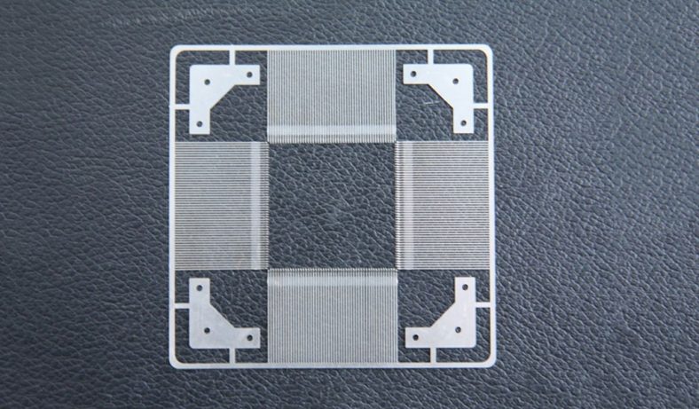
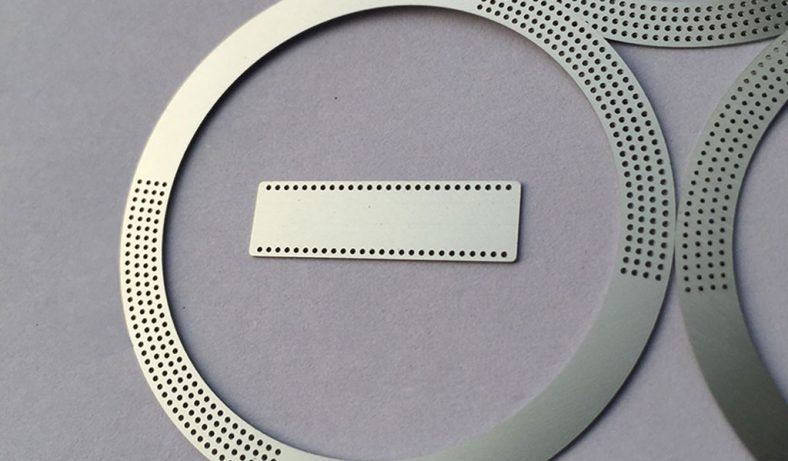
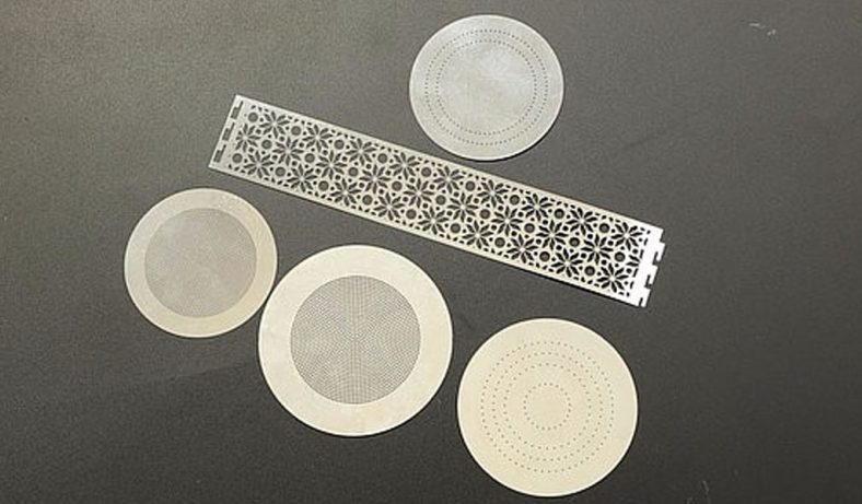
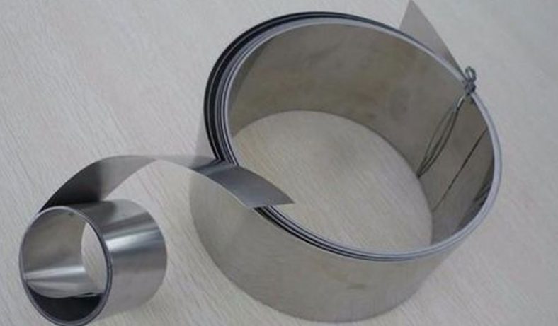
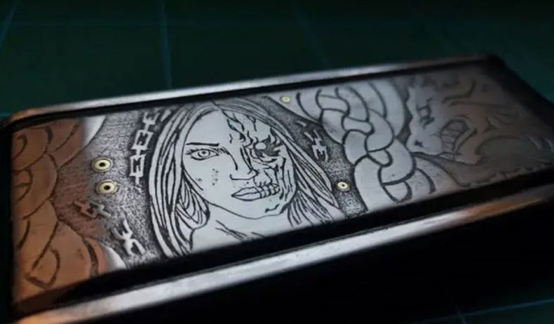
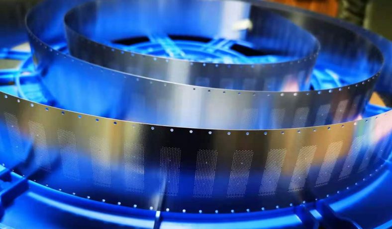
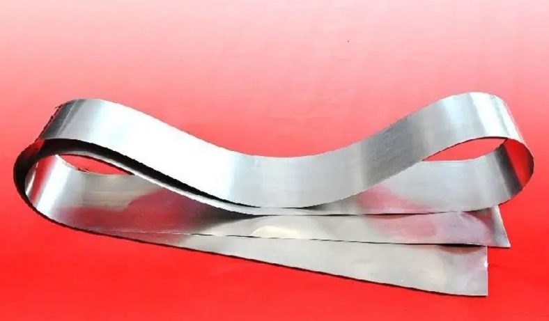
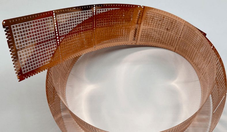
Photolithography and etching are cornerstone processes in the field of micromachining, particularly when applied to materials such as stainless steel, which is widely valued for its mechanical strength, corrosion resistance, and versatility in applications ranging from biomedical devices to aerospace components. Stainless steel micromachining, a subset of microfabrication, involves the creation of intricate, high-precision features on stainless steel substrates at the microscale, typically in the range of micrometers to millimeters. The integration of photolithography and etching has revolutionized the ability to produce complex microstructures with high accuracy, enabling advancements in microelectromechanical systems (MEMS), microfluidics, and precision engineering. This article provides a comprehensive exploration of the process development of photolithography and etching in stainless steel micromachining, detailing historical evolution, technical methodologies, material considerations, and modern advancements. It includes detailed comparative tables to elucidate key parameters and techniques.
Historical Context of Photolithography and Etching
Early Developments in Photolithography
Photolithography, derived from the Greek words “phos” (light), “lithos” (stone), and “graphein” (to write), emerged as a pivotal microfabrication technique in the semiconductor industry during the mid-20th century. Initially developed for integrated circuit (IC) fabrication on silicon substrates, photolithography involves the use of light to transfer geometric patterns from a photomask to a photosensitive material (photoresist) on a substrate. The origins of photolithography can be traced to the 1950s, when researchers at Bell Laboratories, including Jay W. Lathrop and James R. Nall, pioneered the use Photolithography and Etching in Stainless Steel Micromachining
Photolithography and etching are cornerstone processes in the field of micromachining, particularly when applied to materials such as stainless steel, which is widely valued for its mechanical strength, corrosion resistance, and versatility in applications ranging from biomedical devices to aerospace components. Stainless steel micromachining, a subset of microfabrication, involves the creation of intricate, high-precision features on stainless steel substrates at the microscale, typically in the range of micrometers to millimeters. The integration of photolithography and etching has revolutionized the ability to produce complex microstructures with high accuracy, enabling advancements in microelectromechanical systems (MEMS), microfluidics, and precision engineering. This article provides a comprehensive exploration of the process development of photolithography and etching in stainless steel micromachining, detailing historical evolution, technical methodologies, material considerations, and modern advancements. It includes detailed comparative tables to elucidate key parameters and techniques.
Historical Context of Photolithography and Etching
Early Developments in Photolithography
Photolithography, derived from the Greek words “phos” (light), “lithos” (stone), and “graphein” (to write), emerged as a pivotal microfabrication technique in the semiconductor industry during the mid-20th century. Initially developed for integrated circuit (IC) fabrication on silicon substrates, photolithography involves the use of light to transfer geometric patterns from a photomask to a photosensitive material (photoresist) on a substrate. The origins of photolithography can be traced to the 1950s, when researchers at Bell Laboratories, including Jay W. Lathrop and James R. Nall, pioneered the use of photoresist materials to create patterns on silicon wafers. Their work laid the foundation for modern microfabrication, enabling the production of transistors and other microelectronic components.
The adaptation of photolithography to non-semiconductor materials, such as metals like stainless steel, began in the late 20th century as industries sought to leverage the precision of microfabrication for applications beyond electronics. Stainless steel, with its high tensile strength and resistance to harsh environments, posed unique challenges due to its chemical and mechanical properties, necessitating innovations in photoresist application, exposure techniques, and pattern transfer methods.
Evolution of Etching Techniques
Etching, the process of selectively removing material from a substrate to create desired patterns, has been employed for centuries in artistic and industrial contexts. In the context of micromachining, etching techniques were adapted from macroscale metal processing to achieve microscale precision. Early etching methods for metals, including stainless steel, relied on chemical wet etching, where a substrate is immersed in a chemical solution that selectively dissolves material. The introduction of photolithography enabled precise control over etching patterns, as photoresist layers could protect specific areas of the substrate from etchant exposure.
By the 1980s, dry etching techniques, such as plasma etching and reactive ion etching (RIE), emerged as alternatives to wet etching, offering improved resolution and anisotropy (directional etching). These advancements were critical for stainless steel micromachining, where isotropic wet etching often resulted in undercutting and reduced feature fidelity. The combination of photolithography and advanced etching techniques marked a significant milestone in the ability to fabricate complex microstructures on stainless steel.
Fundamentals of Photolithography in Stainless Steel Micromachining
Principles of Photolithography
Photolithography in stainless steel micromachining follows the same fundamental principles as in semiconductor processing but requires adaptations to accommodate the material’s properties. The process begins with the preparation of the stainless steel substrate, which is typically cleaned to remove contaminants such as oils, oxides, or particulates. A thin layer of photoresist, a light-sensitive polymer, is then applied to the substrate, typically through spin coating or lamination. The photoresist is exposed to ultraviolet (UV) light through a photomask, which contains the desired pattern. The exposure alters the chemical properties of the photoresist, rendering it either soluble (positive photoresist) or insoluble (negative photoresist) in a developer solution.
After exposure, the substrate is developed, removing the soluble photoresist regions and leaving a patterned resist layer. This pattern serves as a mask for subsequent etching processes, protecting specific areas of the stainless steel while exposing others to the etchant. The photoresist is later stripped, leaving the etched stainless steel with the desired microstructure.
Photoresist Selection and Application
Selecting an appropriate photoresist is critical for successful photolithography on stainless steel. Positive photoresists, such as those based on diazonaphthoquinone (DNQ), are commonly used due to their high resolution and compatibility with UV exposure systems. Negative photoresists, such as SU-8, are preferred for applications requiring thick resist layers, as they offer excellent mechanical stability and high aspect ratios. The choice of photoresist depends on factors such as feature size, etching method, and substrate adhesion.
Applying photoresist to stainless steel presents challenges due to the material’s smooth, non-porous surface, which can lead to poor adhesion. Surface treatments, such as plasma cleaning or chemical priming with adhesion promoters (e.g., hexamethyldisilazane, HMDS), are often employed to enhance photoresist adhesion. Spin coating is the most common method for applying liquid photoresists, achieving uniform thicknesses ranging from 1 to 100 micrometers. For thicker layers or complex geometries, dry film photoresists, which are laminated onto the substrate, are increasingly used in stainless steel micromachining.
Exposure and Development
Exposure systems for photolithography include contact aligners, proximity aligners, and projection aligners, with contact aligners being the most common for stainless steel micromachining due to their simplicity and cost-effectiveness. The photomask, typically made of glass with a chrome pattern, defines the features to be transferred. The resolution of the photolithographic process is governed by the wavelength of the light source (typically 365–436 nm for UV systems) and the optical properties of the exposure system.
Development involves immersing the exposed substrate in a developer solution, which selectively removes the photoresist based on its exposure state. For positive photoresists, the exposed areas are dissolved, while for negative photoresists, the unexposed areas are removed. The development process must be carefully controlled to avoid over- or under-development, which can compromise pattern fidelity.
Etching Techniques for Stainless Steel Micromachining
Wet Etching
Wet etching is a chemical process that involves immersing the stainless steel substrate in an etchant solution, which selectively removes material from areas not protected by the photoresist mask. Common etchants for stainless steel include ferric chloride (FeCl₃), nitric acid (HNO₃), and hydrochloric acid (HCl), often used in combination to achieve desired etch rates and surface quality. Wet etching is isotropic, meaning it etches equally in all directions, which can lead to undercutting beneath the photoresist mask, limiting the achievable resolution.
The advantages of wet etching include its simplicity, low cost, and ability to process large substrates. However, its isotropic nature makes it less suitable for high-aspect-ratio features or applications requiring precise control over sidewall profiles. The etch rate depends on factors such as etchant concentration, temperature, and the stainless steel alloy composition (e.g., 304, 316L).
Dry Etching
Dry etching, including plasma etching and reactive ion etching (RIE), uses gaseous etchants to remove material. In plasma etching, a plasma of reactive gases (e.g., chlorine-based or fluorine-based gases) is generated, and the reactive species chemically react with the stainless steel surface. RIE combines chemical etching with physical ion bombardment, enhancing anisotropy and enabling vertical sidewall profiles.
Dry etching offers superior resolution and control compared to wet etching, making it ideal for high-precision micromachining. However, it requires sophisticated equipment, such as vacuum chambers and plasma generators, increasing process complexity and cost. The choice of etchant gases depends on the stainless steel alloy and desired etch characteristics, with common gases including Cl₂, BCl₃, and SF₆.
Electrochemical Etching
Electrochemical etching, or electropolishing, is an alternative technique for stainless steel micromachining, particularly for applications requiring smooth surfaces or complex 3D structures. In this process, the stainless steel substrate acts as the anode in an electrolytic cell, and material is removed through controlled dissolution in an electrolyte solution (e.g., phosphoric acid or sulfuric acid). Electrochemical etching can be combined with photolithography to achieve patterned material removal, offering advantages in surface finish and uniformity.
Comparison of Etching Techniques
The choice of etching technique depends on the application requirements, including feature size, aspect ratio, surface quality, and cost. Table 1 provides a detailed comparison of wet etching, dry etching, and electrochemical etching for stainless steel micromachining.
| Parameter | Wet Etching | Dry Etching (RIE) | Electrochemical Etching |
|---|---|---|---|
| Mechanism | Chemical dissolution | Chemical reaction + physical ion bombardment | Electrochemical dissolution |
| Etchant | FeCl₃, HNO₃, HCl | Cl₂, BCl₃, SF₆ | Phosphoric acid, sulfuric acid |
| Anisotropy | Isotropic | Anisotropic | Isotropic |
| Resolution | Moderate (5–20 µm) | High (0.5–5 µm) | Moderate (5–15 µm) |
| Aspect Ratio | Low (≤1:1) | High (up to 10:1) | Moderate (1:1 to 3:1) |
| Surface Finish | Moderate (roughness ~0.5–2 µm) | Good (roughness ~0.1–0.5 µm) | Excellent (roughness <0.1 µm) |
| Equipment Cost | Low | High | Moderate |
| Process Complexity | Simple | Complex | Moderate |
| Applications | Large features, low-cost prototyping | High-precision MEMS, microfluidics | Biomedical devices, smooth surfaces |
Table 1: Comparison of Etching Techniques for Stainless Steel Micromachining
Material Considerations in Stainless Steel Micromachining
Stainless Steel Alloys
Stainless steel is a family of iron-based alloys containing at least 10.5% chromium, which imparts corrosion resistance. Common alloys used in micromachining include 304, 316L, and 17-4PH, each with distinct properties affecting photolithography and etching outcomes. For example, 316L stainless steel, with its higher molybdenum content, offers superior corrosion resistance, making it ideal for biomedical applications, while 17-4PH provides high strength for aerospace components.
The alloy composition influences etch rates, surface roughness, and photoresist adhesion. For instance, high nickel content can enhance resistance to certain etchants, requiring adjustments in etchant selection or process parameters. Table 2 compares key properties of common stainless steel alloys used in micromachining.
| Alloy | Composition (wt%) | Tensile Strength (MPa) | Corrosion Resistance | Etch Rate (Wet, FeCl₃) | Applications |
|---|---|---|---|---|---|
| 304 | Fe, 18–20% Cr, 8–10.5% Ni | 515–620 | Good | Moderate (~1 µm/min) | General-purpose, microfluidics |
| 316L | Fe, 16–18% Cr, 10–14% Ni, 2–3% Mo | 485–550 | Excellent | Slow (~0.5 µm/min) | Biomedical, chemical sensors |
| 17-4PH | Fe, 15–17.5% Cr, 3–5% Ni, 3–5% Cu | 1000–1300 | Moderate | Fast (~1.5 µm/min) | Aerospace, high-strength components |
Table 2: Properties of Stainless Steel Alloys for Micromachining
Surface Preparation
Surface preparation is critical for ensuring photoresist adhesion and etching uniformity. Stainless steel surfaces often contain native oxides or organic contaminants that can interfere with process outcomes. Common cleaning methods include solvent cleaning (e.g., acetone, isopropyl alcohol), ultrasonic cleaning, and plasma cleaning. Surface roughness also plays a role, as highly polished surfaces may reduce photoresist adhesion, while overly rough surfaces can lead to non-uniform etching.
Process Development and Optimization
Photolithography Process Optimization
Optimizing photolithography for stainless steel involves balancing parameters such as photoresist thickness, exposure dose, and development time. Thicker photoresist layers are required for deep etching but may compromise resolution, while thinner layers offer higher resolution but limited etch resistance. Exposure dose must be calibrated to the photoresist type and light source, with overexposure leading to pattern distortion and underexposure resulting in incomplete pattern transfer.
Advanced techniques, such as multi-layer resist systems or grayscale lithography, have been developed to enhance process flexibility. Multi-layer systems involve stacking multiple photoresist layers with different sensitivities, enabling complex 3D structures. Grayscale lithography uses varying exposure doses to create sloped or curved features, which is particularly useful for microfluidic channels or optical components.
Etching Process Optimization
Etching optimization focuses on achieving desired feature geometry, surface quality, and process repeatability. For wet etching, key parameters include etchant concentration, temperature, and agitation. For example, increasing the temperature of a ferric chloride solution from 25°C to 50°C can double the etch rate but may also increase undercutting. Dry etching optimization involves adjusting plasma power, gas flow rates, and chamber pressure to control etch anisotropy and selectivity.
Integration of Photolithography and Etching
The integration of photolithography and etching requires careful process alignment to ensure pattern fidelity. Misalignment between the photomask and substrate can result in distorted features, while variations in photoresist thickness or etching conditions can lead to non-uniform results. Process control techniques, such as statistical process control (SPC) and design of experiments (DOE), are employed to optimize process parameters and minimize variability.
Advanced Techniques and Innovations
Deep Reactive Ion Etching (DRIE)
Deep reactive ion etching (DRIE), a specialized form of RIE, has been adapted for stainless steel micromachining to achieve high-aspect-ratio structures. DRIE alternates between etching and passivation cycles, using gases such as SF₆ for etching and C₄F₈ for sidewall passivation. This “Bosch process” enables vertical sidewalls and aspect ratios exceeding 10:1, making it suitable for applications such as microgears or microfluidic mixers.
Laser-Assisted Etching
Laser-assisted etching combines laser ablation with chemical etching to enhance precision and speed. A laser beam is used to locally heat or ablate the stainless steel surface, facilitating chemical reactions with the etchant. This technique is particularly effective for rapid prototyping or creating complex 3D structures, although it may introduce thermal stress or surface damage.
Multi-Step Processing
Multi-step processing involves combining photolithography and etching with other micromachining techniques, such as laser micromachining or electroforming, to create hybrid structures. For example, a stainless steel substrate may undergo photolithography and etching to define microchannels, followed by electroplating to add functional coatings or structures.
Applications of Photolithography and Etching in Stainless Steel Micromachining
Microelectromechanical Systems (MEMS)
MEMS devices, such as microsensors and microactuators, benefit from the precision of photolithography and etching. Stainless steel MEMS components, such as microvalves or micropumps, leverage the material’s durability and corrosion resistance for applications in harsh environments.
Microfluidics
Microfluidic devices, used in biomedical diagnostics and chemical analysis, rely on stainless steel micromachining to create precise channels and reservoirs. Photolithography and etching enable the fabrication of complex channel networks with feature sizes as small as 1 µm, facilitating applications such as lab-on-a-chip systems.
Biomedical Devices
Stainless steel’s biocompatibility makes it ideal for biomedical applications, including stents, surgical tools, and implantable sensors. Photolithography and etching allow for the creation of intricate features, such as porous surfaces for tissue integration or microelectrodes for neural stimulation.
Aerospace and Automotive Components
In aerospace and automotive industries, stainless steel micromachining is used to fabricate lightweight, high-strength components, such as microgears, fuel injectors, and turbine blades. The precision of photolithography and etching ensures tight tolerances and reliable performance under extreme conditions.
Challenges and Limitations
Material Challenges
Stainless steel’s high mechanical strength and chemical inertness pose challenges for etching, requiring aggressive etchants or high-energy processes. These conditions can degrade photoresist masks or introduce defects, such as pitting or grain boundary etching, particularly in alloys with heterogeneous microstructures.
Process Limitations
The isotropic nature of wet etching limits its use for high-resolution features, while dry etching’s complexity and cost may be prohibitive for low-volume production. Additionally, photolithography on non-planar or curved stainless steel surfaces remains challenging, requiring specialized equipment or techniques.
Scalability and Cost
Scaling photolithography and etching processes for large-scale production of stainless steel microstructures requires significant investment in equipment and process optimization. Balancing cost, throughput, and quality remains a key challenge for industrial applications.
Future Directions
Next-Generation Lithography
Emerging lithography techniques, such as extreme ultraviolet (EUV) lithography and nanoimprint lithography, offer potential for further improving resolution and throughput in stainless steel micromachining. EUV lithography, with wavelengths around 13.5 nm, enables sub-micron feature sizes, while nanoimprint lithography provides a cost-effective alternative for high-volume production.
Advanced Etching Technologies
Advancements in etching technologies, such as atomic layer etching (ALE), promise enhanced precision and control. ALE removes material layer by layer with atomic-scale accuracy, minimizing damage and improving uniformity. These techniques are particularly promising for next-generation MEMS and microfluidic devices.
Integration with Additive Manufacturing
The integration of photolithography and etching with additive manufacturing (e.g., 3D printing) offers new possibilities for creating hybrid stainless steel microstructures. For example, 3D-printed stainless steel scaffolds can be post-processed with photolithography and etching to add microscale features, combining the benefits of both approaches.
Conclusion
Photolithography and etching have transformed stainless steel micromachining, enabling the fabrication of high-precision microstructures for diverse applications. From their origins in semiconductor processing, these techniques have been adapted to overcome the challenges of stainless steel’s unique properties, leading to innovations in MEMS, microfluidics, biomedical devices, and beyond. Ongoing advancements in lithography, etching, and process integration continue to push the boundaries of what is possible, promising even greater precision, scalability, and functionality in the future. The detailed comparison tables provided in this article highlight the key parameters and trade-offs, offering a valuable resource for researchers and engineers in the field.

