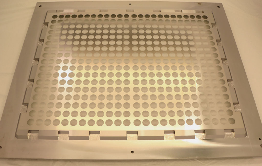
A photomask is an opaque plate with transparent regions used to define the patterns of integrated circuits and other microstructures in the photolithography process. The photomask is a critical component in the semiconductor manufacturing process, as it serves as a template for transferring circuit patterns onto semiconductor wafers, enabling the production of microchips.
History and Development of Photomasks
The photomask is a pivotal component in the photolithography process used in semiconductor manufacturing and other microfabrication applications. Its development has mirrored advancements in technology and manufacturing processes, evolving from simple manual techniques to sophisticated, high-precision devices integral to modern electronics.
Early Beginnings
The origins of photomasks can be traced back to the mid-20th century when the semiconductor industry began to take shape. Early photomasks were created through manual methods and involved transferring circuit designs onto glass plates using photographic techniques. These early masks were relatively crude by modern standards and were used in the early generations of integrated circuits.
The Era of Manual and Photographic Techniques
In the 1960s and 1970s, photomasks were primarily produced using manual drawing techniques. Engineers and designers would create circuit patterns on a transparent film or glass plate, which was then photographed to produce a mask. These early photomasks were limited in resolution and accuracy, which constrained the complexity and miniaturization of integrated circuits.During this period, the photomask industry also saw the introduction of basic photolithographic techniques, where a photographic emulsion was used to transfer patterns onto the mask. The precision and resolution of these early masks were constrained by the technology available at the time.
Advances in Photomask Technology
The 1980s and 1990s marked significant advancements in photomask technology. Key developments included:
Electron Beam Lithography: This technique allowed for higher precision in creating photomasks. Electron beam lithography uses a focused beam of electrons to write the circuit pattern onto a resist-coated substrate. This method greatly improved the resolution and accuracy of photomasks, enabling the production of more complex and miniaturized integrated circuits.
Computer-Aided Design (CAD): The introduction of CAD software revolutionized the design and production of photomasks. CAD allowed engineers to create detailed and accurate circuit designs digitally, which could then be transferred to photomasks with greater precision. This development significantly enhanced the capability to design and fabricate intricate microelectronic circuits.
Improved Materials: Advances in materials science led to the development of new substrate materials for photomasks, such as high-purity quartz. These materials offered better optical properties and durability, which were crucial for high-resolution photolithography.
The Shift to Advanced Lithography Techniques
The late 1990s and early 2000s saw the transition to more advanced photolithography techniques, driven by the need for even smaller feature sizes and greater precision in semiconductor manufacturing. Key innovations included:
- Phase-Shift Masks (PSM): Phase-shift masks were developed to enhance the resolution and contrast of photolithographic imaging. By altering the phase of light passing through different regions of the mask, PSMs improved the ability to print smaller features with greater accuracy.
- Deep Ultraviolet (DUV) Lithography: The shift to DUV lithography, using wavelengths shorter than traditional UV light, enabled the printing of finer features on semiconductor wafers. This advancement required the development of new photomask technologies capable of handling the shorter wavelengths and higher energy levels.
- Attenuated Phase-Shift Masks (Att-PSM): Attenuated phase-shift masks were introduced to improve image contrast while maintaining a high level of transmission. These masks use partially transmissive materials to achieve phase shifting, which enhanced the resolution of dense patterns.
The Modern Era: EUV and Beyond
In the 2010s and beyond, the semiconductor industry continued to push the boundaries of photomask technology to meet the demands of increasingly complex and miniaturized integrated circuits. Key developments include:
- Extreme Ultraviolet (EUV) Lithography: The introduction of EUV lithography represented a major leap forward in photomask technology. EUV lithography uses extremely short wavelengths of light, around 13.5 nm, to print features at the scale of a few nanometers. EUV masks are highly complex and require specialized materials and fabrication techniques to withstand the high-energy photons used in the process.
- Computational Lithography: Advanced computational methods, such as inverse lithography and machine learning algorithms, have been integrated into the photomask design and fabrication process. These techniques enhance pattern fidelity and reduce defects, enabling the production of even smaller and more intricate features.
- Directed Self-Assembly (DSA): Directed self-assembly is an emerging technique that complements traditional photomask-based lithography. DSA leverages the self-organizing properties of certain materials to create patterns at the nanoscale, potentially offering new ways to achieve high-resolution patterning.
- Environmental Considerations: There is an increasing focus on developing environmentally friendly photomask manufacturing processes. Efforts are being made to reduce the use of hazardous chemicals, improve energy efficiency, and minimize the environmental impact of photomask production.
The history and development of photomasks reflect the broader advancements in semiconductor technology and microfabrication. From early manual techniques to sophisticated, high-precision devices, photomasks have played a crucial role in enabling the miniaturization and complexity of modern integrated circuits. As the industry continues to innovate and push the boundaries of technology, photomasks will remain a vital component in the fabrication of cutting-edge electronic devices.
Types of Photomasks
Photomasks are integral to the photolithography process used in semiconductor manufacturing and other microfabrication applications. They come in various types, each tailored to specific applications and technologies. Understanding the different types of photomasks is crucial for grasping their roles and functionalities in the production of microelectronic devices.
1. Binary Masks
Binary masks are the most basic type of photomasks, consisting of opaque and transparent regions that correspond directly to the circuit design. They are made from a quartz or glass substrate with a thin layer of opaque material, typically chromium or iron oxide.
- Structure: Binary masks have two distinct regions: opaque (blocking light) and transparent (allowing light to pass through).
- Applications: These masks are suitable for simpler circuit designs and lower-resolution applications. They are used in various semiconductor and microfabrication processes but have limitations in terms of resolution and depth of focus.
2. Phase-Shift Masks (PSM)
Phase-shift masks enhance the resolution and depth of focus in the photolithography process by altering the phase of light passing through different regions of the mask. This phase shift improves image contrast and allows for the printing of finer features.
- Structure: PSMs have regions that shift the phase of the transmitted light by 180 degrees. This phase shift enhances the contrast between the printed features and the background.
- Applications: PSMs are used in high-resolution lithography applications where improved pattern definition is required. They are particularly useful in advanced semiconductor manufacturing and photonic device fabrication.
3. Attenuated Phase-Shift Masks (Att-PSM)
Attenuated phase-shift masks use partially transmissive materials to achieve phase shifting. Unlike binary masks, which either block or transmit light, Att-PSMs allow a fraction of light to pass through, resulting in improved image contrast without completely blocking the light.
- Structure: Att-PSMs have regions with attenuated (partially blocked) transmission, which allows for a controlled phase shift.
- Applications: These masks are used in applications where enhanced contrast is needed without the need for full phase shift. They are common in high-resolution lithography processes where fine patterning is required.
4. Alternating Phase-Shift Masks (Alt-PSM)
Alternating phase-shift masks utilize alternating phase shifts of 180 degrees between adjacent features. This technique improves the resolution and definition of dense patterns by enhancing the contrast between neighboring features.
- Structure: Alt-PSMs alternate between regions that shift the light phase by 0 degrees and 180 degrees. This alternating pattern enhances the resolution and sharpness of printed features.
- Applications: These masks are particularly useful for printing dense and complex patterns in advanced semiconductor devices and high-resolution imaging applications.
5. Extreme Ultraviolet (EUV) Masks
Extreme ultraviolet (EUV) masks are designed for EUV lithography, which uses extremely short wavelengths of light (around 13.5 nm) to print features at the nanoscale. EUV masks are highly specialized and require advanced materials and fabrication techniques.
- Structure: EUV masks consist of a multilayer coating that reflects EUV light, a high-precision substrate, and a protective pellicle. The multilayer coating is typically made of alternating layers of molybdenum and silicon.
- Applications: EUV masks are used in cutting-edge semiconductor manufacturing processes to achieve extremely fine feature sizes and high-resolution patterning.
6. Design-Rule Check (DRC) Masks
Design-rule check masks are used to verify that semiconductor designs adhere to specific design rules and constraints. These masks are typically employed during the design phase to ensure that the patterns and features meet manufacturing requirements.
- Structure: DRC masks are designed to highlight potential design rule violations by overlaying test patterns and measurements.
- Applications: These masks are used primarily in the design verification and validation stages of semiconductor manufacturing.
7. High-NA Masks
High numerical aperture (NA) masks are used in photolithography systems with high numerical aperture optics, which allow for greater resolution and finer patterning. These masks are designed to work with advanced lithography tools that use high-NA lenses to achieve superior image quality.
- Structure: High-NA masks are engineered to match the specifications of high-NA lithography tools, including precise optical characteristics and pattern alignment.
- Applications: They are used in advanced semiconductor manufacturing processes where high resolution and precision are critical.
Each type of photomask serves a specific purpose in the photolithography process, with variations designed to address different challenges and requirements in semiconductor manufacturing and microfabrication. From basic binary masks to advanced EUV masks, the choice of photomask type is crucial for achieving the desired resolution, contrast, and accuracy in the production of integrated circuits and other microelectronic devices. As technology continues to advance, photomasks will continue to evolve, incorporating new materials and techniques to meet the demands of increasingly complex and miniaturized electronic devices.
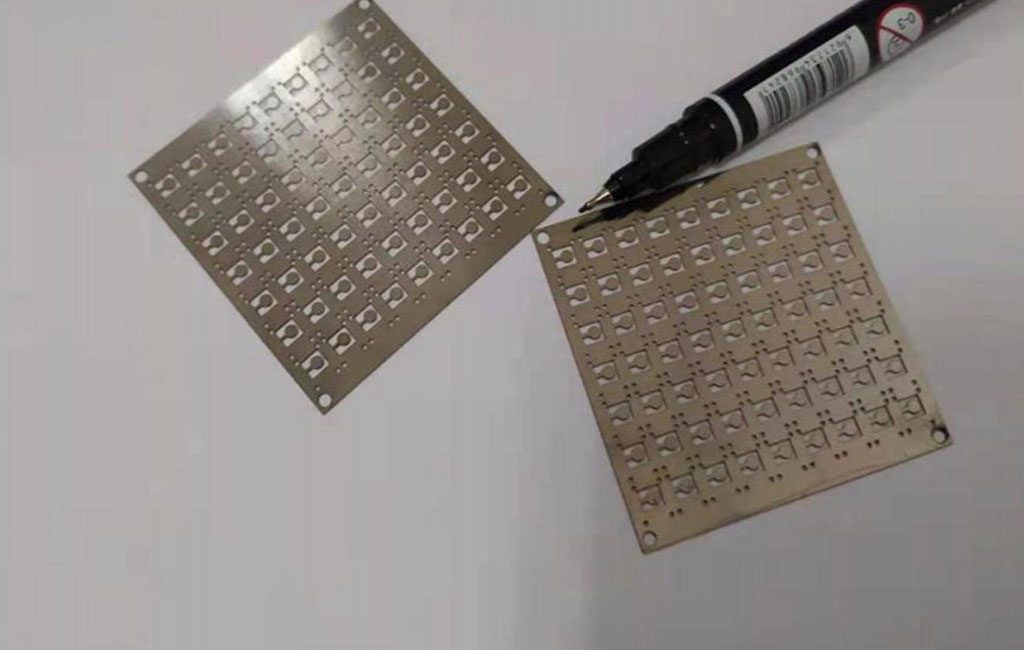
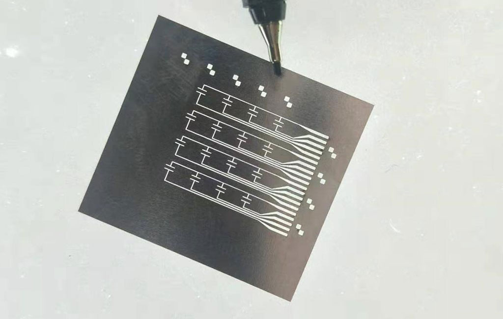
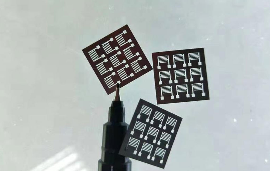
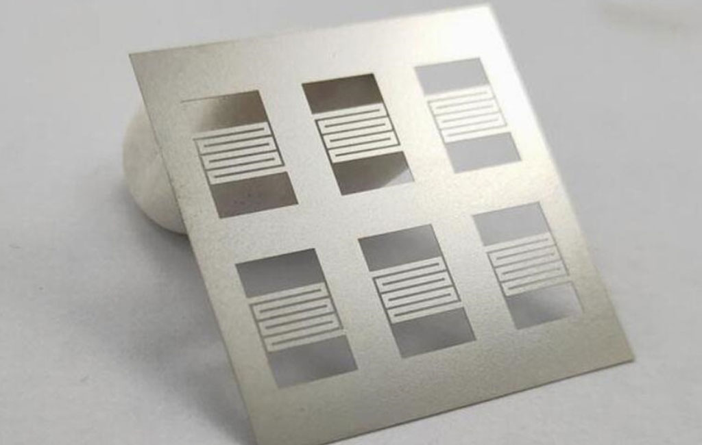
Photomask Fabrication: How to Etch a Photomask
Photomask fabrication is a critical process in the production of integrated circuits and microstructures. Etching is a key step in this process, involving the transfer of intricate circuit patterns onto a photomask substrate.
Overview of Photomask Fabrication
Photomask fabrication typically involves several stages, including design, substrate preparation, coating, exposure, development, and etching. The etching process specifically transfers the circuit pattern from a photosensitive layer to the underlying substrate.
Steps in Photomask Etching
1. Design and Pattern Generation
The process begins with the creation of a detailed circuit design using Computer-Aided Design (CAD) software. The design is converted into a format suitable for photomask production, usually in the form of a digital file that specifies the patterns to be etched.
2. Substrate Preparation
The photomask substrate is usually made from high-purity quartz or glass. The substrate must be meticulously cleaned to remove any contaminants or particles that could affect the quality of the final mask.
- Cleaning: The substrate is cleaned using solvents and deionized water to ensure it is free from dust, oils, and other impurities. This step may include ultrasonic cleaning and chemical treatments.
3. Coating with Photosensitive Material
A photosensitive resist layer is applied to the substrate. This resist material reacts to light exposure, allowing the creation of patterns.
- Photoresist Application: The substrate is coated with a thin layer of photoresist, typically using spin coating, where the resist is spread evenly across the surface as the substrate spins at high speeds.
- Soft Bake: The coated substrate is then baked at a low temperature to remove solvents from the resist and improve its adhesion to the substrate.
4. Exposure
The photoresist-coated substrate is exposed to light through a photomask or mask aligner. The light exposure transfers the circuit pattern onto the photoresist layer.
- Exposure Tool: An electron beam (e-beam) or optical lithography system is used to expose the photoresist to the light pattern. This process creates a latent image of the circuit pattern in the photoresist.
5. Development
After exposure, the substrate is developed to remove the unexposed or exposed photoresist, depending on whether a positive or negative resist is used.
- Developing Solution: The substrate is immersed in a developing solution that dissolves either the exposed or unexposed photoresist, revealing the circuit pattern on the substrate.
- Rinsing and Drying: The substrate is then rinsed with deionized water and dried to remove any remaining developing solution.
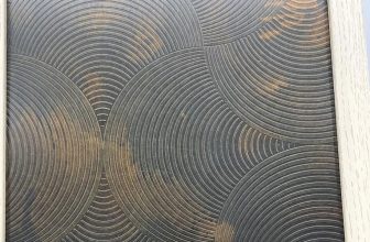
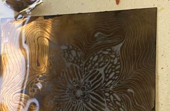
6. Etching
Etching is the process of removing material from the substrate to transfer the pattern from the photoresist layer to the substrate. There are several etching techniques used in photomask fabrication:
Wet Etching
Process: Wet etching involves immersing the substrate in a chemical solution that selectively removes material from the exposed areas. The solution is carefully chosen to etch the material beneath the photoresist while leaving the photoresist intact.
Advantages: Wet etching is simpler and cost-effective for certain materials.
Disadvantages: It can be less precise due to the isotropic nature of the etching process, which can lead to undercutting and loss of feature resolution.
Dry Etching
Process: Dry etching uses plasma or reactive gases to etch the substrate material. This method includes several techniques:
Reactive Ion Etching (RIE): RIE uses a plasma of reactive gases to etch the substrate in a controlled manner, offering better resolution and anisotropy compared to wet etching.
Deep Reactive Ion Etching (DRIE): DRIE is a specialized form of RIE that enables high aspect ratio etching, suitable for creating deep and narrow features.
Ion Beam Etching (IBE): IBE uses a focused beam of ions to etch the substrate, providing high precision and control.
Advantages: Dry etching offers higher resolution, better feature control, and anisotropic etching, which minimizes undercutting and maintains feature fidelity.
Disadvantages: Dry etching is more complex and expensive compared to wet etching.
7. Photoresist Removal
After etching, the remaining photoresist must be removed to reveal the final pattern on the substrate.
- Photoresist Strip: The substrate is treated with a photoresist stripper or solvent to remove the remaining photoresist material, leaving only the etched pattern on the substrate.
- Final Cleaning: The substrate undergoes a final cleaning process to remove any residual chemicals or particles.
8. Inspection and Repair
The etched photomask is inspected using high-resolution microscopy and metrology tools to ensure it meets the required specifications. Any defects or imperfections are repaired using focused ion beam (FIB) technology or other repair techniques.
- Inspection: Automated and manual inspection methods are used to detect defects such as pattern deviations, particles, or contamination.
- Repair: Defects are corrected using techniques such as FIB milling or deposition to restore the mask’s integrity.
9. Pellicle Application
To protect the photomask from contamination during use, a pellicle—a thin, transparent membrane—is applied to the surface.
Pellicle Application: The pellicle is carefully aligned and affixed to the photomask to ensure it does not interfere with the optical patterning process.
The etching process in photomask fabrication is a critical step that transfers intricate circuit patterns onto the photomask substrate. By using a combination of photoresist coating, exposure, development, and etching techniques, manufacturers can achieve high-resolution and precise patterns required for advanced semiconductor devices. The choice of etching method—wet or dry—depends on the desired resolution, feature size, and material characteristics. As technology continues to advance, innovations in photomask fabrication techniques will further enhance the capabilities and applications of photomasks in semiconductor manufacturing and beyond.
Applications of Photomasks
Photomasks are essential tools in the photolithography process, crucial for various high-precision manufacturing applications. They are primarily used to transfer intricate patterns onto substrates, enabling the production of semiconductor devices, microelectromechanical systems (MEMS), and other microfabricated components. Here’s a detailed overview of their key applications:
1. Semiconductor Manufacturing
Semiconductor manufacturing is the most significant application of photomasks. They are used to define and transfer circuit patterns onto silicon wafers in the production of integrated circuits (ICs).
- Integrated Circuits (ICs): Photomasks are used to create the multiple layers of intricate patterns required for modern ICs, including transistors, capacitors, and interconnections. As semiconductor technology advances, photomasks must accommodate increasingly smaller feature sizes and more complex designs.
- Process Nodes: With the continuous push towards smaller process nodes (e.g., 5 nm, 3 nm), photomasks are crucial for achieving the high resolution and precision needed for advanced semiconductor devices.
2. Microelectromechanical Systems (MEMS)
Microelectromechanical systems (MEMS) integrate mechanical and electrical components on a single chip, used in various applications including sensors, actuators, and microfluidics.
- Sensors: MEMS sensors, such as accelerometers and gyroscopes, rely on photomasks to define the microstructures that detect physical changes or movements.
- Actuators: MEMS actuators, used in applications like inkjet printers and optical switches, are fabricated using photomasks to create precise mechanical components.
3. Flat-Panel Displays
Flat-panel displays, such as liquid crystal displays (LCDs) and organic light-emitting diode (OLED) displays, use photomasks in the production of thin-film transistors (TFTs) and other key components.
- Thin-Film Transistors (TFTs): Photomasks are used to pattern the thin-film transistors that control the pixels in LCDs and OLED displays, ensuring accurate display functionality and high resolution.
- Color Filters: In color LCDs, photomasks are employed to create color filters that produce the desired colors and enhance the display’s image quality.
4. Printed Circuit Boards (PCBs)
Printed circuit boards (PCBs) are fundamental to electronic devices, providing the physical platform for electrical connections between components.
- Patterning Traces: Photomasks are used to define the intricate copper traces and pads on PCBs, enabling the precise routing of electrical signals and power distribution.
- Multilayer PCBs: For complex, multilayer PCBs, photomasks are used to create the detailed patterns required for each layer, ensuring accurate alignment and functionality of the final board.
5. Optoelectronics
Optoelectronics involves the integration of optical and electronic components, such as photonic devices and optical sensors.
- Photonic Devices: Photomasks are used to fabricate components like waveguides, optical filters, and modulators, which are critical for telecommunications and data communication systems.
- Optical Sensors: Devices such as image sensors and light detectors are manufactured using photomasks to create precise optical elements and circuitry.
6. Microfluidics
Microfluidics involves the manipulation of fluids on a microscale, with applications in lab-on-a-chip devices and biomedical diagnostics.
- Lab-on-a-Chip: Photomasks are used to fabricate microchannels and other fluidic components on lab-on-a-chip devices, enabling complex biochemical analyses and assays in a compact format.
- Biomedical Devices: In biomedical applications, photomasks are employed to create microstructures for diagnostic assays, drug delivery systems, and tissue engineering.
7. Nanotechnology
Nanotechnology involves the manipulation of materials at the nanometer scale, with applications in advanced materials and nanodevices.
- Nanostructures: Photomasks are used to pattern nanoscale features in various nanotechnology applications, including nanostructured materials, nanoelectronics, and nanophotonics.
- Nanofabrication: In nanofabrication processes, photomasks help define the precise patterns needed to create nanoscale devices and structures.
8. Lithography Research and Development
Lithography research and development involves the creation and testing of new photolithographic techniques and materials.
- Experimental Masks: Researchers use photomasks to explore new lithography methods, such as extreme ultraviolet (EUV) lithography and directed self-assembly (DSA), and to develop innovative materials and processes.
- Prototype Development: Photomasks are employed in the development of prototype devices and systems, allowing researchers to validate and refine new technologies before full-scale production.
Photomasks are versatile tools with a wide range of applications across various fields, from semiconductor manufacturing to nanotechnology. Their ability to precisely transfer patterns onto substrates enables the production of complex electronic devices, microstructures, and optical components. As technology continues to evolve, the role of photomasks will remain pivotal in advancing the capabilities and applications of modern electronics and microfabrication technologies.