Precision etching, a highly specialized manufacturing technique, has emerged as a cornerstone of modern military technology, enabling the production of intricate, high-performance components critical to defense applications. This process, rooted in advanced materials science and engineering, involves the selective removal of material from a substrate—typically metal, semiconductor, or ceramic—using chemical, physical, or combined methods to achieve precise geometries and tolerances. In the context of military use, precision etching plays an indispensable role in fabricating components for weapons systems, sensors, communication devices, and advanced platforms such as drones, satellites, and missile guidance systems. Its ability to produce complex, lightweight, and reliable parts with minimal mechanical stress has made it a preferred method in the defense sector, where performance, durability, and precision are non-negotiable.
The origins of precision etching can be traced back to early chemical etching processes used in the electronics industry during the mid-20th century, particularly for creating printed circuit boards (PCBs). However, its evolution into a military-grade technology began with the advent of more sophisticated methods, such as photochemical etching (PCE), reactive ion etching (RIE), and laser etching, which offered unprecedented control over material removal at micro- and nanoscale levels. These techniques have since been adapted and refined to meet the stringent requirements of military applications, where components must withstand extreme environmental conditions—such as high temperatures, pressures, and vibrations—while maintaining operational integrity. The versatility of precision etching lies in its ability to work with a wide range of materials, including metals like titanium, aluminum, and stainless steel, as well as semiconductors like silicon and gallium arsenide, which are foundational to military electronics.
At its core, precision etching relies on the principle of selective material removal. In chemical-based methods, an etchant—a corrosive substance, typically an acid or base—is applied to a masked substrate, dissolving exposed areas while leaving masked regions intact. Physical methods, such as plasma-based etching, use ionized gases to bombard the surface, removing material through momentum transfer. Hybrid approaches, like RIE, combine chemical and physical mechanisms to achieve greater anisotropy (directional control) and precision. For military purposes, this level of control is critical, as it allows engineers to fabricate components with intricate features—such as microfluidic channels, high-aspect-ratio trenches, and burr-free edges—that are essential for advanced systems like radar arrays, thermal management devices, and microelectromechanical systems (MEMS).
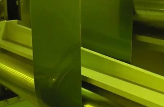
One of the most widely used precision etching techniques in military manufacturing is photochemical etching, also known as chemical milling or photoetching. This process begins with the application of a photoresist—a light-sensitive polymer—onto a metal substrate, typically a thin sheet of alloy such as stainless steel, copper, or titanium. The photoresist is then exposed to ultraviolet (UV) light through a photomask, which defines the desired pattern by hardening the exposed areas. After development, the unexposed photoresist is washed away, leaving a protective mask over the substrate. The exposed metal is then etched using a chemical solution, such as ferric chloride for steel or cupric chloride for copper, which dissolves the unprotected areas. The result is a component with precise features, often as thin as 0.0003 inches (0.0076 mm) and with tolerances as tight as ±0.001 inches (0.0254 mm).
Photochemical etching offers several advantages for military applications. First, it is a low-temperature process, meaning it introduces minimal thermal stress or distortion to the material—a critical factor for components like missile fins, antenna arrays, and heat sinks, which must maintain structural integrity under operational loads. Second, it produces burr-free edges, eliminating the need for secondary finishing processes that could introduce defects or increase production costs. Third, the process is highly scalable, allowing for rapid prototyping as well as large-scale production of identical parts, a necessity for outfitting military fleets with standardized components. For example, photochemical etching has been used to manufacture precision shims and gaskets for aircraft engines, where even minor deviations in thickness could compromise performance.
Another key etching technique in military use is reactive ion etching, which has become a staple in the fabrication of semiconductor-based devices. RIE employs a plasma—a partially ionized gas—generated in a vacuum chamber by applying radiofrequency (RF) energy to a process gas, such as sulfur hexafluoride (SF₆) or tetrafluoromethane (CF₄). The plasma produces reactive species (e.g., fluorine radicals) that chemically react with the substrate, while ions accelerated by an electric field physically bombard the surface, enhancing etch rates and anisotropy. A notable advancement in RIE is the Bosch process, a deep reactive ion etching (DRIE) method that alternates between etching (using SF₆) and passivation (using octafluorocyclobutane, C₄F₈) cycles to create high-aspect-ratio structures in silicon. This technique is particularly valuable for military MEMS devices, such as accelerometers and gyroscopes used in inertial navigation systems.
The Bosch process exemplifies the level of precision required for military applications. By depositing a thin polymer layer on the sidewalls during the passivation step, it prevents lateral etching, allowing trenches with aspect ratios exceeding 50:1 (depth-to-width) to be achieved. For instance, a trench 500 micrometers deep and 10 micrometers wide—a feat unachievable with traditional wet etching—can be etched into a silicon wafer with near-vertical sidewalls. Such structures are integral to the miniaturization of military electronics, enabling the development of compact, lightweight sensors for unmanned aerial vehicles (UAVs) and wearable soldier systems. The ability to etch silicon with such precision has also facilitated the integration of MEMS with microelectronics, creating hybrid systems that combine sensing, processing, and actuation on a single chip.
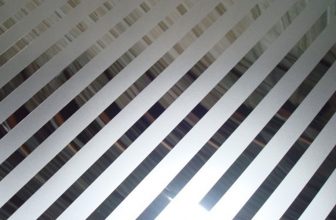
Laser etching, another precision technique, uses focused beams of light to ablate or vaporize material from a substrate. Unlike chemical methods, laser etching is a dry process, requiring no liquid etchants or masks, which simplifies production and reduces waste. Modern systems employ pulsed lasers, such as femtosecond or picosecond lasers, to minimize heat-affected zones (HAZ) and achieve sub-micrometer resolution. In military contexts, laser etching is used to engrave identification markings on weapon components, fabricate microfluidic devices for chemical detection, and create optical elements like diffraction gratings for laser-based targeting systems. Its non-contact nature makes it ideal for processing delicate or heat-sensitive materials, such as polymers and ceramics, which are increasingly used in advanced composites for armor and radomes.
The military applications of precision etching are vast and diverse, spanning land, air, sea, and space domains. In aerospace, etched components are critical to the performance of jet engines, satellites, and hypersonic vehicles. For example, titanium fuel injector nozzles, etched with micron-scale orifices, enhance combustion efficiency in fighter aircraft, while aluminum heat exchangers with etched microchannels improve thermal management in radar systems. In naval systems, precision-etched stainless steel filters and screens are used in submarine propulsion systems to remove contaminants from seawater, ensuring reliable operation during extended missions. On the ground, etched MEMS sensors in smart munitions enable real-time trajectory adjustments, increasing accuracy and reducing collateral damage.
One of the most transformative applications of precision etching is in the realm of military electronics, particularly for communication and surveillance systems. Antennas fabricated through photochemical etching, such as conformal arrays on flexible substrates, allow for lightweight, low-profile designs that can be integrated into soldier helmets or vehicle surfaces. Similarly, RIE-etched silicon waveguides and photonic circuits underpin advanced radar and lidar systems, providing high-resolution imaging for target detection. The ability to etch features smaller than 1 micrometer has also enabled the production of quantum dot-based detectors, which offer enhanced sensitivity to infrared radiation—a critical capability for night vision and missile tracking.
Precision etching’s role in weaponry cannot be overstated. The development of precision-guided munitions (PGMs), such as the Joint Direct Attack Munition (JDAM), relies on etched components like gyroscopes and control surfaces to achieve pinpoint accuracy. For instance, a photochemically etched beryllium copper flexure in a missile’s guidance system allows for minute adjustments in flight, ensuring the weapon strikes within meters of its intended target. In directed-energy weapons, such as high-energy lasers, etched optical components—mirrors, lenses, and beam splitters—must maintain surface flatness to within nanometers to focus energy effectively. These examples underscore how precision etching bridges the gap between theoretical design and battlefield performance.
To understand the comparative advantages of precision etching techniques in military use, it is useful to examine their performance metrics alongside alternative manufacturing methods, such as mechanical machining, stamping, and additive manufacturing (3D printing). Table 1 provides a detailed comparison based on key parameters: resolution, material compatibility, production speed, cost, and stress induction.
| Technique | Resolution (μm) | Material Compatibility | Production Speed | Cost per Unit (Relative) | Stress Induction |
|---|---|---|---|---|---|
| Photochemical Etching | 25–100 | Metals (e.g., Ti, Al, SS, Cu) | Moderate (batch) | Low–Moderate | Minimal |
| Reactive Ion Etching | 0.1–10 | Semiconductors (e.g., Si, GaAs) | Slow (sequential) | High | Low |
| Laser Etching | 0.5–50 | Metals, ceramics, polymers | Fast (sequential) | Moderate–High | Low–Moderate |
| Mechanical Machining | 50–500 | Metals, some ceramics | Moderate (sequential) | Moderate | High |
| Stamping | 100–1000 | Metals (ductile) | Fast (batch) | Low | High |
| Additive Manufacturing | 50–200 | Metals, polymers | Slow (sequential) | High | Moderate |
Table 1: Comparison of Precision Etching and Alternative Manufacturing Techniques for Military Applications
Photochemical etching excels in producing thin, flat components with moderate resolution and low cost, making it ideal for mass production of items like shims, filters, and antenna elements. Its minimal stress induction is a significant advantage over mechanical machining and stamping, which can introduce residual stresses that weaken components under cyclic loading—a common scenario in military environments. RIE, with its sub-micrometer resolution, is unmatched for semiconductor-based devices but is slower and more expensive, limiting its use to high-value, low-volume applications like MEMS. Laser etching offers versatility and speed, though its cost and potential for localized heating make it less suitable for large-scale production of metal parts.
Recent advancements in precision etching have further expanded its military utility. As of March 17, 2025, research into atomic layer etching (ALE)—a variant of RIE that removes material one atomic layer at a time—has shown promise for fabricating next-generation nanoscale devices. ALE’s extreme precision, with etch rates as low as 0.1 nanometers per cycle, enables the creation of transistors and sensors with unprecedented performance, such as ultra-low-power electronics for autonomous drones. Similarly, advancements in laser technology, including the use of extreme ultraviolet (EUV) lasers, have improved resolution to below 10 nanometers, facilitating the production of optical components for space-based surveillance systems.
The integration of artificial intelligence (AI) and machine learning (ML) into etching processes represents another frontier. AI-driven process control can optimize etch parameters—such as gas flow, plasma power, and exposure time—in real time, reducing variability and improving yield. For military manufacturers, this translates to faster development cycles and higher reliability, critical for maintaining technological superiority. For example, an AI-optimized Bosch process could dynamically adjust passivation cycles to compensate for substrate imperfections, ensuring consistent trench depths across a wafer.
Material science innovations have also enhanced precision etching’s capabilities. The development of advanced alloys, such as nickel-titanium (Nitinol) and cobalt-chromium, has expanded the range of etchable materials, enabling the production of shape-memory components for actuators and resilient springs for cryogenic systems. Likewise, the etching of graphene and other two-dimensional (2D) materials has opened new possibilities for flexible electronics, such as wearable sensors that monitor soldier vitals or detect chemical agents. These materials, etched with techniques like plasma-enhanced chemical vapor deposition (PECVD), offer exceptional strength-to-weight ratios and conductivity, aligning with the military’s push for lightweight, multifunctional systems.
The environmental and logistical challenges of precision etching in military contexts warrant consideration. Chemical etching processes, while effective, generate hazardous waste—such as spent etchants and photoresist residues—that must be managed under strict regulations, such as the U.S. Resource Conservation and Recovery Act (RCRA). Military facilities often employ closed-loop systems to recycle etchants, reducing waste and cost. Dry etching methods like RIE and laser etching, which produce minimal liquid waste, are increasingly favored for their sustainability, though they require significant energy inputs for plasma generation or laser operation. Balancing performance, cost, and environmental impact remains an ongoing challenge for defense contractors.
Precision etching’s role in military innovation is evident in specific case studies. The U.S. Department of Defense (DoD), through partnerships with companies like Northrop Grumman and Lockheed Martin, has leveraged photochemical etching to produce radar-absorbing meshes for stealth aircraft. These meshes, etched from copper-clad laminates, feature hexagonal patterns with sub-millimeter apertures that dissipate electromagnetic waves, reducing the aircraft’s radar cross-section. Similarly, RIE-etched silicon carbide (SiC) substrates have been used in high-power amplifiers for satellite communications, offering superior thermal conductivity and breakdown voltage compared to traditional silicon.
The global landscape of precision etching for military use reflects a competitive race for technological dominance. China, for instance, has invested heavily in RIE and DRIE capabilities as part of its “Made in China 2025” initiative, aiming to produce indigenous MEMS and photonic devices for its military. Chinese firms like Ziyan have integrated etched components into autonomous drones, such as the Blowfish A2, which boasts AI-driven targeting and reconnaissance functions. In contrast, the United States maintains a lead in laser etching and ALE, supported by robust funding from DARPA (Defense Advanced Research Projects Agency) and a strong industrial base. European nations, notably Germany and France, contribute through advancements in photochemical etching for aerospace, with companies like Precision Micro supplying etched parts for NATO platforms.
To quantify the performance of etched components in military systems, Table 2 compares key metrics for three representative applications: a missile guidance flexure (photochemical etching), a MEMS gyroscope (RIE), and an optical grating (laser etching).
| Component | Technique | Material | Feature Size (μm) | Tolerance (μm) | Max Operating Temp (°C) | Weight (g) |
|---|---|---|---|---|---|---|
| Missile Guidance Flexure | Photochemical | BeCu | 50 | ±5 | 200 | 0.5 |
| MEMS Gyroscope | RIE (Bosch) | Si | 2 | ±0.1 | 150 | 0.01 |
| Optical Grating | Laser | Fused Silica | 1 | ±0.05 | 1000 | 2.0 |
Table 2: Performance Metrics of Precision-Etched Military Components
The missile guidance flexure, made from beryllium copper (BeCu), demonstrates photochemical etching’s ability to produce lightweight, flexible parts with moderate precision, suitable for dynamic environments. The MEMS gyroscope, etched via the Bosch process, achieves exceptional resolution and tolerance, critical for navigation accuracy in GPS-denied scenarios. The laser-etched optical grating, crafted from fused silica, withstands extreme temperatures, making it ideal for laser weapon systems.
Looking ahead, precision etching is poised to evolve with emerging military needs. The rise of hypersonic weapons, which travel at speeds exceeding Mach 5, demands components with enhanced thermal and mechanical properties. Etched ceramic matrix composites (CMCs), capable of withstanding temperatures above 2000°C, are under development to meet these requirements. Similarly, the push for quantum technologies—such as quantum radar and cryptography—relies on etched nanostructures, like quantum wells and photonic crystals, to manipulate light and matter at the atomic scale. These advancements will require further refinements in etching resolution, possibly through hybrid techniques combining ALE and EUV lithography.
The economic implications of precision etching in military manufacturing are significant. While initial setup costs for RIE and laser systems can exceed $1 million, their ability to produce high-value components offsets this investment over time. Photochemical etching, with lower capital costs (typically $50,000–$100,000 for equipment), offers a cost-effective alternative for mass production, with per-unit costs as low as $0.10 for simple parts like washers. The DoD’s 2025 budget allocates approximately $2.3 billion for advanced manufacturing R&D, including etching technologies, reflecting their strategic importance.
In conclusion, precision etching stands as a linchpin of military technology, enabling the fabrication of components that define modern warfare. Its scientific foundation—spanning chemistry, physics, and materials engineering—underpins its versatility and precision, while ongoing innovations ensure its relevance in an era of rapid technological change. As of March 17, 2025, the interplay of photochemical etching, RIE, and laser etching continues to shape military capabilities, from stealth and precision strikes to autonomous systems and beyond. Through detailed comparisons and real-world applications, this article has illuminated the critical role of precision etching in defending national interests and advancing human ingenuity.