Precision etching is a highly specialized manufacturing process used to selectively remove material from a substrate with exceptional accuracy and control. This technique plays a pivotal role in industries such as microelectronics, aerospace, medical device fabrication, and nanotechnology, where intricate patterns, fine tolerances, and high-quality finishes are paramount. Unlike traditional machining methods that rely on mechanical force, precision etching employs chemical, physical, or combined processes to achieve results at microscopic or even nanoscopic scales. The versatility of precision etching allows it to be applied to a wide range of materials, including metals, semiconductors, ceramics, and polymers, making it an indispensable tool in modern engineering and technology.
The origins of etching can be traced back to the Middle Ages, when artisans used acid solutions to decorate metal armor and weapons with intricate designs. However, the development of precision etching as a scientific and industrial process emerged in the 20th century, driven by the demands of the electronics industry for creating miniaturized circuits. Today, precision etching encompasses a variety of techniques, each tailored to specific applications and material properties. These methods include wet chemical etching, dry plasma etching, laser etching, and electrochemical etching, among others. This article provides a comprehensive, step-by-step exploration of precision etching techniques, detailing the processes, tools, materials, and considerations involved, along with comparative analyses to elucidate their differences and applications.
Step 1: Understanding the Fundamentals of Etching
Before delving into the procedural aspects of precision etching, it is essential to grasp the underlying principles that govern the process. Etching involves the controlled removal of material from a substrate, typically achieved by exposing the material to a reactive agent—be it a chemical solution, plasma gas, or focused energy beam. The goal is to create patterns or features with precise dimensions, often guided by a mask or template that defines the areas to be etched.
The substrate, or workpiece, is the material being etched, and its properties—such as composition, crystal structure, and thickness—significantly influence the etching process. Common substrates include silicon wafers in semiconductor manufacturing, stainless steel in medical implants, and glass in optical components. The etching agent, known as the etchant, is selected based on its reactivity with the substrate and its ability to achieve the desired etch rate and selectivity. Selectivity refers to the etchant’s preference for removing the target material over the mask or underlying layers, a critical factor in achieving high precision.
Etching can be isotropic or anisotropic. Isotropic etching occurs uniformly in all directions, resulting in rounded or undercut features, while anisotropic etching is directional, producing sharp, well-defined structures. The choice between isotropic and anisotropic etching depends on the application; for instance, microelectromechanical systems (MEMS) often require anisotropic etching to create vertical sidewalls, whereas decorative etching may favor isotropic profiles for smoother contours.
Step 2: Preparing the Substrate
The first practical step in precision etching is preparing the substrate to ensure optimal results. This stage is crucial, as any surface imperfections, contaminants, or inconsistencies can compromise the etching process and the quality of the final product. Substrate preparation typically involves cleaning, surface treatment, and, in some cases, the application of a base layer.
Cleaning is performed to remove organic residues, dust, oxides, or other impurities from the substrate surface. For example, in semiconductor manufacturing, silicon wafers are cleaned using the RCA process, a multi-step method involving solutions of ammonium hydroxide, hydrogen peroxide, and hydrochloric acid. This ensures a pristine surface free of particulates that could interfere with subsequent steps. For metal substrates like copper or aluminum, degreasing with solvents such as acetone or isopropyl alcohol may be employed, followed by acid rinsing to remove oxide layers.
Surface treatment may also include polishing or planarization to achieve a uniform thickness and smoothness, particularly for applications requiring sub-micron precision. In some cases, a thin adhesion layer—such as titanium or chromium—is deposited onto the substrate to enhance the bonding of subsequent layers, such as a photoresist mask.
Step 3: Applying the Mask
The mask is a critical component of precision etching, serving as a stencil that defines the pattern to be etched into the substrate. The mask protects specific areas of the substrate from the etchant while exposing others, allowing for selective material removal. Masks can be temporary, such as photoresists used in photolithography, or permanent, such as metal hard masks employed in deep reactive ion etching (DRIE).
In photolithography, a common masking technique, a light-sensitive polymer called photoresist is applied to the substrate via spin coating, creating a uniform layer typically 1–10 micrometers thick. The photoresist is then exposed to ultraviolet (UV) light through a photomask—a glass plate with a patterned opaque coating—using a mask aligner. The exposed areas of the photoresist undergo a chemical change, becoming either soluble (positive resist) or insoluble (negative resist) in a developer solution. After development, the unexposed or exposed regions (depending on the resist type) are washed away, leaving a patterned mask on the substrate.
For applications requiring greater durability, such as etching deep features into silicon, a hard mask made of materials like silicon dioxide (SiO₂) or silicon nitride (Si₃N₄) may be used. These masks are deposited using techniques like chemical vapor deposition (CVD) and patterned via a separate etching step before the main substrate etch begins.
Step 4: Selecting the Etching Technique
With the substrate prepared and masked, the next step is selecting the appropriate etching technique. The choice depends on factors such as the material, desired feature size, etch depth, sidewall profile, and production scale. Below, we explore the major precision etching methods in detail.
Wet Chemical Etching
Wet chemical etching involves immersing the masked substrate in a liquid etchant that chemically reacts with the exposed material. Common etchants include hydrofluoric acid (HF) for silicon dioxide, nitric acid (HNO₃) for metals like copper, and potassium hydroxide (KOH) for silicon. The process is typically isotropic, though anisotropic etching can be achieved with certain crystalline materials and etchants, such as KOH on silicon, which etches faster along specific crystal planes (e.g., <100> versus <111>).
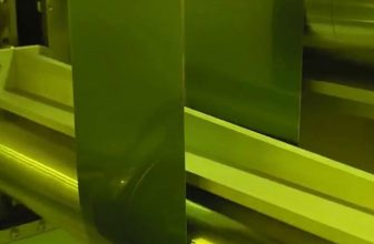
The procedure begins by placing the substrate in an etchant bath, often temperature-controlled to regulate the etch rate. Agitation may be applied to ensure uniform etching and prevent bubble formation, which can cause defects. Once the desired etch depth is achieved, the substrate is removed, rinsed with deionized water to stop the reaction, and dried. Wet etching is cost-effective and suitable for large-scale production but lacks the precision of dry methods for sub-micron features due to undercutting.
Dry Plasma Etching
Dry plasma etching, also known as reactive ion etching (RIE), uses a plasma—a partially ionized gas—to remove material. The process occurs0 occurs in a vacuum chamber where gases like sulfur hexafluoride (SF₆) or chlorine (Cl₂) are introduced and energized by radiofrequency (RF) power, generating reactive ions and radicals. These species bombard the substrate, combining chemical reactions with physical sputtering to etch the exposed areas.
RIE offers greater control over anisotropy and selectivity compared to wet etching, making it ideal for microelectronics. The substrate is placed on an electrode within the plasma chamber, and parameters such as gas flow, pressure, and RF power are adjusted to optimize the etch profile. Advanced variants like deep reactive ion etching (DRIE), used in MEMS, alternate etching and passivation cycles (e.g., SF₆ for etching and C₄F₈ for sidewall protection) to achieve high-aspect-ratio structures.
Laser Etching
Laser etching employs a focused laser beam to ablate material from the substrate surface. Techniques like laser micromachining use pulsed lasers, such as excimer or femtosecond lasers, to vaporize material with minimal thermal damage. The substrate is mounted on a precision stage, and the laser is directed by computer-controlled optics to trace the desired pattern.
This method excels at etching complex, non-repetitive patterns on delicate materials like glass or polymers, where chemical methods might be too aggressive. However, it is slower and less scalable than plasma or wet etching, making it better suited for prototyping or small-batch production.
Electrochemical Etching
Electrochemical etching combines chemical reactions with an electric current to remove material. The substrate acts as an anode in an electrolyte bath, and a cathode completes the circuit. When voltage is applied, metal ions dissolve from the substrate into the solution, creating features determined by the mask. This technique is widely used for etching metals like stainless steel or titanium in medical device manufacturing.
Step 5: Executing the Etch
With the technique selected, the etching process is executed under controlled conditions. For wet etching, the substrate is submerged in the etchant for a calculated duration based on the etch rate, which is determined experimentally or from literature (e.g., HF etches SiO₂ at ~100 nm/min at room temperature). In plasma etching, the substrate is loaded into the chamber, and the plasma is ignited, with real-time monitoring via optical emission spectroscopy to track reaction byproducts. Laser etching involves programming the beam path and adjusting pulse energy, while electrochemical etching requires tuning the voltage and current density.
Throughout the etch, parameters are monitored to ensure uniformity and prevent over-etching, which could damage underlying layers or alter feature dimensions. In some cases, in-situ metrology tools, such as ellipsometry or interferometry, are used to measure etch depth without interrupting the process.
Step 6: Post-Etching Processing
Once etching is complete, the substrate undergoes post-processing to remove the mask, clean the surface, and inspect the results. For photoresist masks, a solvent like acetone or a plasma ashing process (using O₂ plasma) strips the resist without damaging the substrate. Hard masks may require a separate etch, such as HF for SiO₂. Cleaning removes etchant residues and particulates, often using deionized water, ultrasonic baths, or mild acids.
Inspection is conducted using tools like scanning electron microscopy (SEM), atomic force microscopy (AFM), or profilometry to verify feature dimensions, sidewall angles, and surface roughness. If defects such as over-etching, under-etching, or mask misalignment are detected, the process parameters are adjusted, and the step may be repeated on a new substrate.
Step 7: Optimization and Iteration
Precision etching is an iterative process, requiring optimization to meet stringent specifications. Factors like etchant concentration, temperature, plasma power, or laser intensity are fine-tuned based on inspection results. Test runs on dummy substrates help establish a repeatable process before scaling to production. Statistical process control (SPC) may be employed to monitor variability and ensure consistency across batches.
Comparative Analysis of Etching Techniques
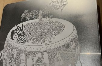
Precision etching underpins numerous technologies. In microelectronics, it fabricates integrated circuits with features as small as 2 nm. In MEMS, it creates sensors and actuators for automotive and medical applications. Aerospace components benefit from lightweight, high-strength parts etched from titanium or composites. Medical implants, such as stents, rely on etched patterns for biocompatibility and functionality. Even art and jewelry use etching for intricate designs on metals and gemstones.
Below are detailed tables comparing the major precision etching techniques across key parameters.
| Technique | Mechanism | Materials | Precision (Feature Size) | Anisotropy | Scalability |
|---|---|---|---|---|---|
| Wet Chemical Etching | Chemical reaction | Metals, semiconductors, glass | 1–10 μm | Low–Moderate | High |
| Dry Plasma Etching | Chemical + Physical | Semiconductors, dielectrics | 10 nm–1 μm | High | Moderate–High |
| Laser Etching | Ablation | Metals, polymers, ceramics | 1–50 μm | High | Low–Moderate |
| Electrochemical Etching | Electrochemical dissolution | Metals | 10–100 μm | Moderate | Moderate |
| Technique | Key Parameters | Control Method | Typical Etch Rate | Mask Type |
|---|---|---|---|---|
| Wet Chemical Etching | Etchant concentration, temperature | Bath immersion, agitation | 10–1000 nm/min | Photoresist, hard mask |
| Dry Plasma Etching | Gas flow, RF power, pressure | Plasma chamber monitoring | 1–100 nm/min | Hard mask, photoresist |
| Laser Etching | Pulse energy, beam focus | CNC optics | 0.1–10 μm/pass | None or software mask |
| Electrochemical Etching | Voltage, current density | Power supply adjustment | 1–50 μm/min | Photoresist, hard mask |
| Technique | Advantages | Limitations |
|---|---|---|
| Wet Chemical Etching | Simple, low-cost, high throughput | Isotropic, limited precision |
| Dry Plasma Etching | High precision, anisotropic | Expensive equipment, complex setup |
| Laser Etching | Non-contact, versatile materials | Slow, thermal effects possible |
| Electrochemical Etching | Metal-specific, moderate cost | Limited material range, slower rates |
Conclusion
Precision etching faces challenges such as maintaining uniformity over large areas, minimizing environmental impact (e.g., from toxic etchants like HF), and pushing feature sizes below 1 nm for next-generation electronics. Emerging techniques, such as atomic layer etching (ALE), promise atomic-scale precision by removing material one atomic layer at a time. Hybrid methods combining wet and dry etching or laser-assisted plasma etching are also being explored to balance speed, cost, and accuracy.
Precision etching is a cornerstone of modern manufacturing, enabling the creation of intricate, high-performance components across diverse fields. By following the step-by-step process—substrate preparation, masking, technique selection, execution, post-processing, and optimization—engineers can tailor the method to specific needs. With ongoing advancements, precision etching continues to evolve, driving innovation in technology and beyond.