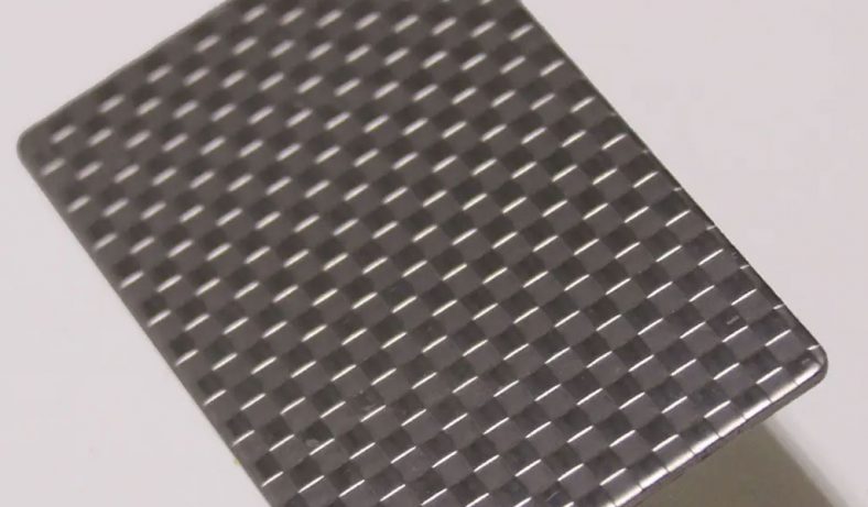
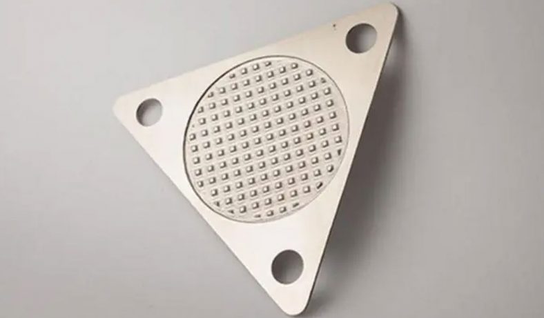
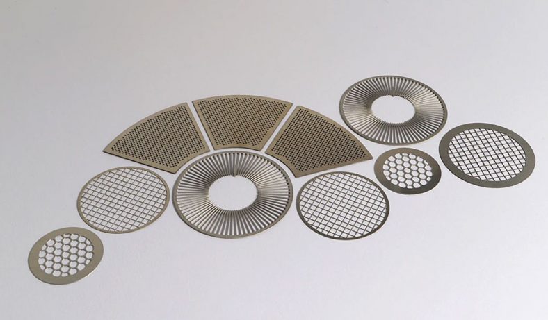
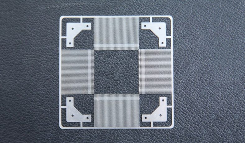
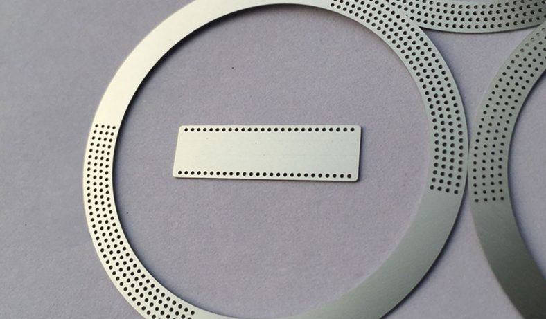
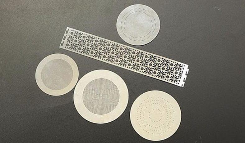
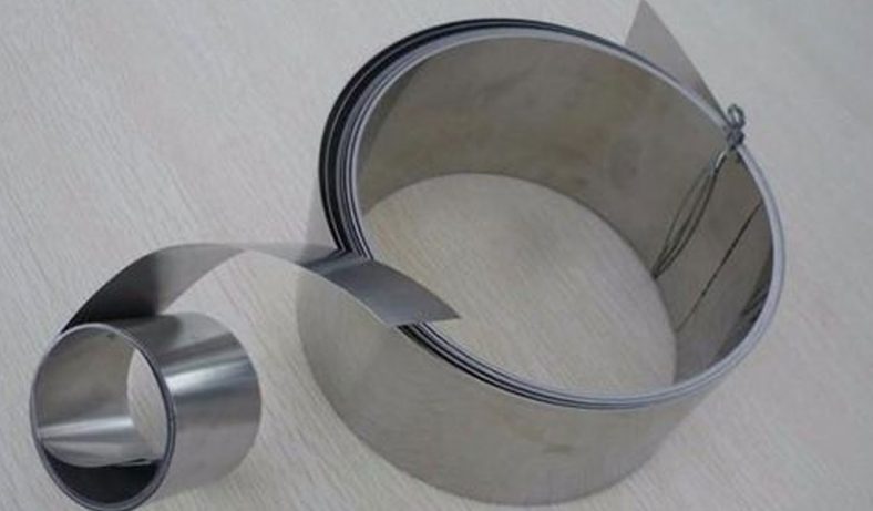
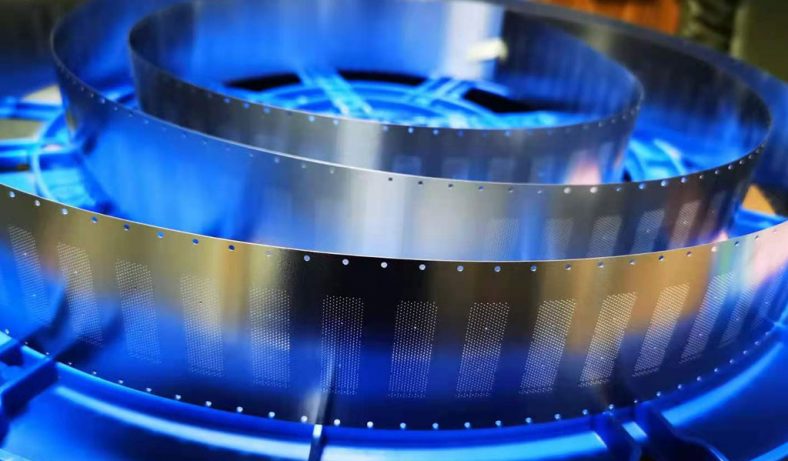
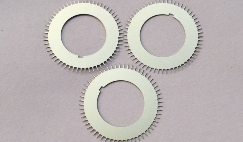
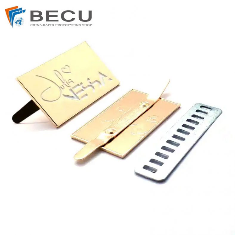
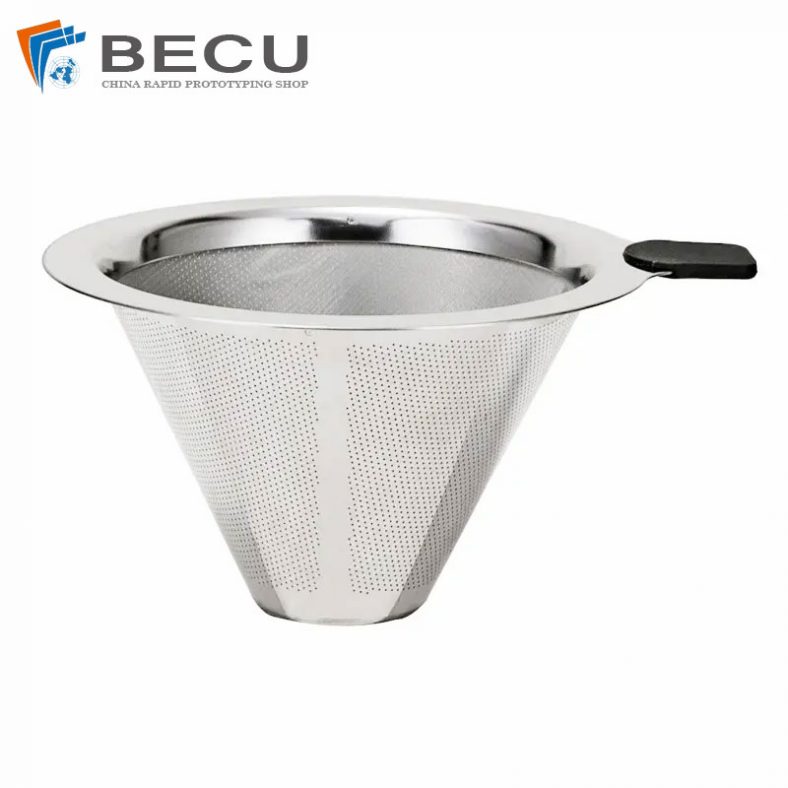
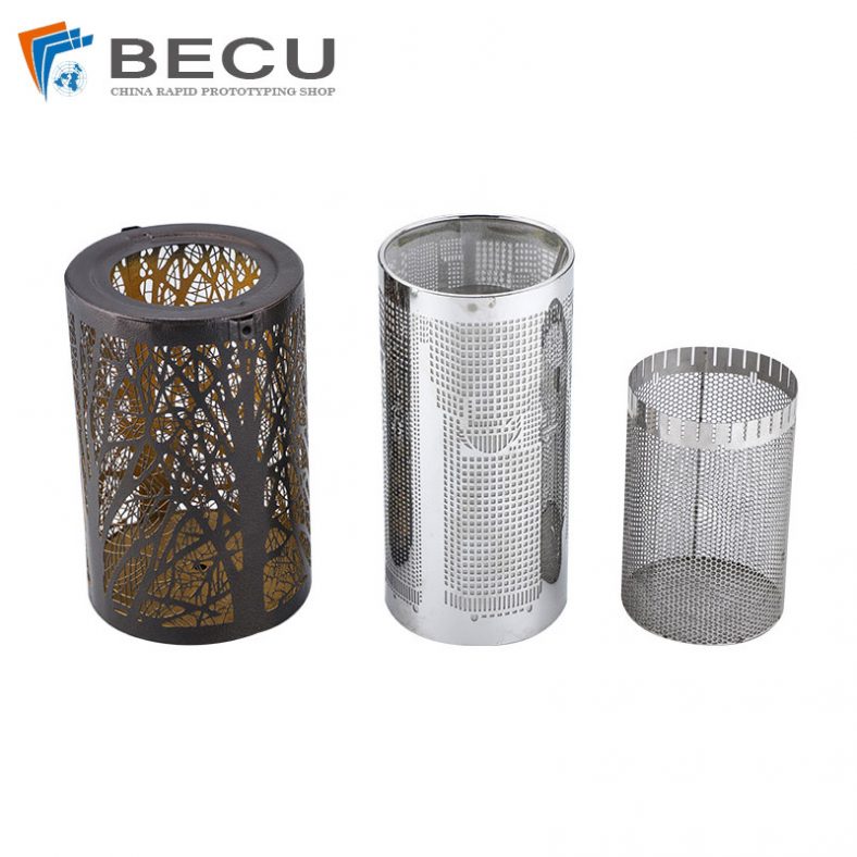
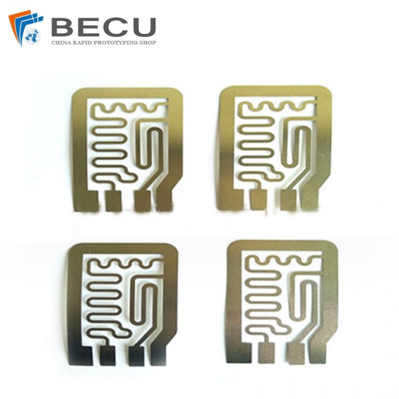
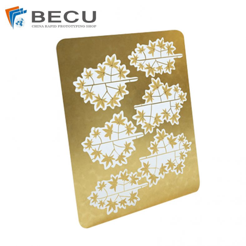
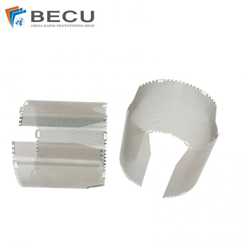
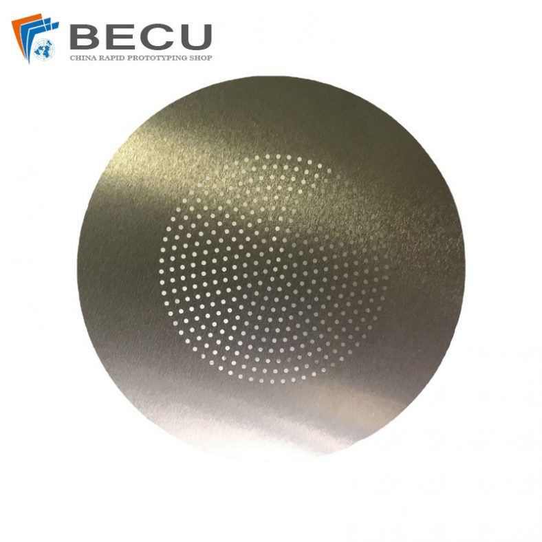
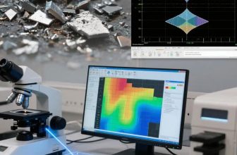
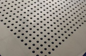
Photochemical etching, also known as photochemical machining (PCM) or chemical etching, is a subtractive manufacturing process that employs chemical etchants and photoresist masks to fabricate intricate, high-precision metal components. This technique is particularly valuable in micro-nano processing, where the demand for components with submicron accuracy and complex geometries has surged across industries such as electronics, aerospace, medical devices, and renewable energy. Among the materials processed, zinc alloys have emerged as a critical substrate due to their corrosion resistance, ductility, and suitability for die-casting applications. Recent advancements in photochemical etching have significantly enhanced its precision, enabling the production of zinc alloy components with unprecedented accuracy at micro and nanoscale dimensions.
This article explores the mechanisms, advancements, and applications of photochemical etching in zinc alloy micro-nano processing, with a focus on precision improvements. It examines the historical context, technical principles, material properties, process optimizations, and emerging trends, supported by detailed comparisons and data. The discussion is structured to provide a comprehensive, scientific overview, drawing on recent studies and industry practices to elucidate the transformative potential of this technology.
Historical Context of Photochemical Etching
Photochemical etching originated in the 1960s as an offshoot of the printed circuit board industry, initially developed to fabricate copper-based circuits with high precision. The process leveraged photographic techniques to create patterns on metal surfaces, which were then selectively etched using chemical solutions. Over decades, the technique evolved to accommodate a broader range of metals, including stainless steel, aluminum, titanium, and zinc alloys. The transition to micro-nano processing began in the late 20th century, driven by the miniaturization demands of electronics and microelectromechanical systems (MEMS).
Zinc alloys, composed primarily of zinc with elements such as aluminum, copper, and magnesium, gained prominence in photochemical etching due to their favorable mechanical and chemical properties. Early applications focused on decorative components and corrosion-resistant coatings, but the advent of micro-nano processing expanded their use to precision parts like microfluidic channels, sensors, and optical gratings. The challenge of achieving submicron precision in zinc alloys spurred innovations in etchant formulations, photoresist technologies, and process controls, setting the stage for modern advancements.
Principles of Photochemical Etching
Process Overview
Photochemical etching involves several sequential steps to transform a metal sheet into a precision component:
- Substrate Preparation: A zinc alloy sheet, typically 0.01 to 2.0 mm thick, is cleaned to remove surface contaminants, ensuring uniform adhesion of the photoresist.
- Photoresist Application: A photosensitive polymer (photoresist) is applied to both sides of the sheet, forming a thin, uniform layer.
- Pattern Exposure: A photographic mask, or photo-tool, containing the desired component design is aligned over the photoresist-coated sheet. Ultraviolet (UV) light is projected through the mask, hardening the exposed photoresist areas.
- Development: Unexposed photoresist is removed using a developer solution, revealing the underlying zinc alloy in areas to be etched.
- Etching: The sheet is exposed to a chemical etchant, typically an aqueous solution of ferric chloride or ammonium chloride, which selectively dissolves the exposed metal. The photoresist protects unetched areas, preserving the design.
- Stripping and Finishing: The remaining photoresist is stripped away, and the etched component is cleaned, inspected, and, if necessary, subjected to secondary processes like forming or coating.
Chemical and Physical Mechanisms
The etching process relies on a controlled chemical reaction between the etchant and the zinc alloy. Ferric chloride (FeCl₃), a common etchant, reacts with zinc to form soluble zinc chloride (ZnCl₂):
[ \text{Zn} + 2\text{FeCl}_3 \rightarrow \text{ZnCl}_2 + 2\text{FeCl}_2 ]
This reaction is highly anisotropic when optimized, allowing for precise material removal. The etch rate, typically 0.013–0.025 mm per minute per side, depends on factors such as etchant concentration, temperature, and agitation. Ammonium chloride (NH₄Cl) is often preferred for zinc oxide (ZnO) films due to its controllable etch rate and linear behavior, critical for nanoscale applications.
The photoresist serves as a protective mask, with its resolution determining the minimum feature size. Modern dry film and liquid photoresists achieve resolutions below 0.1 mm, enabling the creation of microscale features. The non-contact, non-thermal nature of photochemical etching eliminates mechanical stresses and thermal distortions, ensuring burr-free, smooth surfaces—a significant advantage over traditional machining methods like stamping or laser cutting.
Zinc Alloys in Micro-Nano Processing
Material Properties
Zinc alloys are versatile materials with properties that make them ideal for photochemical etching:
- Corrosion Resistance: Zinc naturally forms a protective oxide layer, enhancing durability in harsh environments.
- Ductility and Malleability: Alloys like Zamak (zinc with aluminum, magnesium, and copper) exhibit excellent formability, facilitating post-etching processes like bending or deep drawing.
- Electrical Conductivity: Zinc alloys, particularly those with copper, are suitable for electronic components such as connectors and shielding.
- Recyclability: Zinc is highly recyclable, aligning with sustainable manufacturing practices.
Common zinc alloys used in photochemical etching include:
- Zamak 3: A general-purpose alloy with 4% aluminum, offering good strength and castability.
- Zamak 5: Contains 1% copper for enhanced strength and hardness.
- Nickel-Silver (Cu-Ni-Zn): A copper-zinc-nickel alloy used for EMI/RFI shielding due to its solderability and nonmagnetic properties.
Challenges in Zinc Alloy Etching
Despite their advantages, zinc alloys present challenges in micro-nano processing:
- Surface Porosity: High etch rates can increase surface roughness, affecting precision.
- Alloy Variability: Variations in alloy composition (e.g., aluminum or copper content) influence etch uniformity.
- Etchant Sensitivity: Zinc’s reactivity requires precise control of etchant chemistry to avoid over-etching or undercutting.
Recent advancements have addressed these challenges through optimized etchant formulations, advanced photoresists, and real-time process monitoring.
Advancements in Precision Improvement
Etchant Optimization
The precision of photochemical etching hinges on the etchant’s ability to remove material uniformly and predictably. Recent studies have focused on tailoring etchant compositions for zinc alloys:
- Ammonium Chloride Solutions: Research demonstrates that NH₄Cl provides near-linear etch rates for zinc oxide films, with etchant concentration and temperature significantly affecting outcomes. For instance, a 2022 study found that a 1 M NH₄Cl solution at 40°C achieved an etch rate of 0.5 nm/s with minimal surface roughness.
- Additives: Isopropyl alcohol (IPA) and surfactants improve surface quality by reducing bubble formation and enhancing wettability, minimizing defects like pitting.
- pH Control: Maintaining a stable pH (typically 4–6) prevents unwanted side reactions, ensuring consistent etch profiles.
Photoresist Technology
Advancements in photoresist materials have enhanced resolution and durability:
- High-Resolution Dry Films: Modern dry film photoresists achieve feature sizes as small as 0.05 mm, compared to 0.1 mm for earlier generations. These films withstand prolonged exposure to etchants, critical for deep etching.
- Liquid Photoresists: Liquid photoresists offer superior conformality for complex geometries, enabling nanoscale patterns. A 2024 study reported a liquid photoresist achieving a 50 nm line width on zinc oxide films.
- Multi-Layer Resists: Stacked photoresist layers improve etch depth control, allowing for high-aspect-ratio structures.
Process Control and Automation
Precision improvements owe much to advanced process control:
- Real-Time Monitoring: Spectroscopic and laser-based systems monitor etch rates and surface quality in situ, enabling dynamic adjustments to etchant flow and temperature.
- Automated Spray Systems: Multi-chamber etching machines with arrays of spray nozzles ensure uniform etchant distribution, reducing variability across large sheets.
- Statistical Process Optimization: Statistical methods, such as those applied to zinc oxide etching, identify dominant factors (e.g., temperature, concentration) and their interactions, optimizing etch rate and selectivity. A 2022 study used factorial design to achieve a 20% improvement in etch uniformity.
Comparison of Etching Techniques
The following table compares photochemical etching with other micro-nano processing methods for zinc alloys:
| Parameter | Photochemical Etching | Laser Etching | Reactive Ion Etching (RIE) | Stamping |
|---|---|---|---|---|
| Minimum Feature Size (µm) | 50 | 10 | 5 | 100 |
| Aspect Ratio | Up to 10:1 | 20:1 | 100:1 | 5:1 |
| Material Stress | None | Moderate (thermal) | Low | High |
| Burr Formation | None | Minimal | None | Common |
| Tooling Cost | Low (~$350) | High | High | Very High |
| Processing Time | Hours | Minutes | Hours | Seconds |
| Material Versatility | High (most metals) | Moderate | Low (semiconductors) | High |
| Environmental Impact | Moderate (chemicals) | Low | High (vacuum systems) | Low |
Table 1: Comparison of Micro-Nano Processing Techniques for Zinc Alloys
Photochemical etching excels in cost-effectiveness and material versatility, though it lags behind RIE in achievable aspect ratios. Its burr-free, stress-free nature makes it ideal for precision applications.
Applications in Micro-Nano Processing
Electronics
Zinc alloys, particularly nickel-silver, are widely used in electronics for EMI/RFI shielding, connectors, and lead frames. Photochemical etching enables the production of microscale features like 0.1 mm slots and fold lines, critical for compact devices. The process’s ability to etch thin metals (0.01–0.25 mm) supports the miniaturization trend in smartphones, wearables, and IoT devices.
Medical Devices
In medical applications, zinc alloys are etched to create stents, catheters, and surgical instruments. The biocompatibility of zinc oxide and the precision of photochemical etching allow for microchannels and intricate patterns in lab-on-a-chip devices. A 2023 study highlighted the use of etched zinc alloy microfluidic plates in diagnostic tools, achieving channel widths below 100 µm.
Renewable Energy
Zinc oxide thin films are critical in thin-film silicon solar cells, where textured surfaces enhance light trapping. Chemical etching of ZnO films, optimized for etch rate and selectivity, produces nanoscale textures that improve conversion efficiency. A 2011 study reported a 15% efficiency gain using etched ZnO surfaces.
Aerospace and Automotive
In aerospace, etched zinc alloy components like turbine blades and heat exchangers benefit from the process’s ability to create complex geometries without thermal stress. In automotive applications, fuel cell plates and precision gaskets leverage photochemical etching’s cost-effectiveness and repeatability.
Emerging Trends and Future Directions
Metal-Assisted Chemical Etching (MACE)
Metal-assisted chemical etching (MACE) is an emerging technique that enhances photochemical etching’s precision for nanoscale applications. MACE uses a metal catalyst (e.g., gold or silver) to induce electrochemical reactions, enabling the formation of high-aspect-ratio nanostructures. A 2024 review highlighted MACE’s ability to achieve aspect ratios exceeding 100:1 in silicon, with potential applications in zinc oxide-based sensors.
Hybrid Processes
Combining photochemical etching with other techniques, such as laser micromachining or additive manufacturing, offers new possibilities. For instance, laser pre-patterning can enhance photoresist resolution, while 3D-printed molds guide etchant flow for 3D microstructures. These hybrid approaches are under active investigation for zinc alloy processing.
Sustainable Practices
Environmental concerns have driven innovations in etchant recycling and water conservation. Precision Micro reported recycling 35% of water used in its etching processes in 2022, alongside using 100% renewable energy. Future developments aim to reduce chemical waste through closed-loop systems and biodegradable etchants.
Artificial Intelligence and Machine Learning
AI and machine learning are transforming process optimization. Predictive models analyze etchant performance, photoresist behavior, and surface quality, reducing trial-and-error. A 2025 study demonstrated a 30% reduction in defect rates using AI-driven etching parameters for zinc alloys.
Challenges and Limitations
Despite its advancements, photochemical etching faces limitations:
- Thickness Constraints: The process is best suited for thin sheets (<2.5 mm), limiting its use for bulk components.
- Feature Size Limits: While 50 µm features are achievable, sub-10 µm patterns require costly equipment or hybrid techniques.
- Chemical Waste: Etchant disposal remains a concern, though recycling efforts mitigate impacts.
- Scalability: Large-scale production may be less cost-effective compared to stamping for simple geometries.
Addressing these challenges requires continued investment in materials science, process engineering, and sustainable technologies.
Conclusion
Photochemical etching has undergone significant advancements, positioning it as a cornerstone of zinc alloy micro-nano processing. Improvements in etchant formulations, photoresist technologies, and process controls have elevated precision, enabling feature sizes below 50 µm and aspect ratios up to 10:1. Zinc alloys, with their corrosion resistance and ductility, are ideal substrates for applications in electronics, medical devices, renewable energy, and aerospace. Emerging trends like MACE, hybrid processes, and AI-driven optimization promise further enhancements, while sustainable practices address environmental concerns.

