Potassium dihydrogen phosphate (KDP) crystals are widely used in various optical applications due to their exceptional nonlinear optical properties. These crystals are particularly valuable in high-power laser systems, where they are employed for frequency conversion and electro-optic switching. The performance and longevity of KDP crystals are significantly influenced by the quality of their processing surfaces. Subsurface damage (SSD) is a critical issue that can degrade the optical performance and reduce the lifespan of these crystals. This article delves into the detection and analysis of subsurface damage in KDP crystal processing surfaces, providing a comprehensive overview of the techniques, methodologies, and scientific principles involved.
Understanding Subsurface Damage
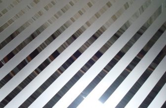
Subsurface damage refers to the microscopic defects and cracks that occur beneath the surface of a material during processing. In the context of KDP crystals, SSD can arise from various mechanical and chemical processes, including cutting, polishing, and etching. These defects can lead to reduced optical transmission, increased scattering, and degraded laser damage threshold. Understanding the mechanisms behind SSD is crucial for developing effective detection and mitigation strategies.
Mechanisms of Subsurface Damage
The formation of SSD in KDP crystals can be attributed to several mechanisms:
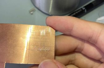
- Mechanical Stress: During cutting and polishing, mechanical stresses can induce micro-cracks and dislocations within the crystal lattice. These stresses can propagate through the material, leading to deeper subsurface defects.
- Chemical Etching: Chemical processes used to clean or modify the surface of KDP crystals can also introduce SSD. Etching solutions can penetrate the surface and react with the crystal, creating microscopic pits and voids.
- Thermal Effects: High-energy processes, such as laser cutting or thermal annealing, can cause localized heating and cooling, leading to thermal stresses and subsequent SSD.
- Environmental Factors: Exposure to humidity, temperature fluctuations, and other environmental factors can exacerbate SSD by promoting the growth of existing defects.
Detection Techniques
Detecting SSD in KDP crystals requires advanced analytical techniques that can probe beneath the surface. Several methods are commonly employed:
- Optical Microscopy: Traditional optical microscopy can provide initial insights into surface defects, but its resolution is limited to the surface layer. Advanced techniques like confocal microscopy can offer better depth resolution.
- Scanning Electron Microscopy (SEM): SEM provides high-resolution images of the surface and subsurface regions. By using backscattered electron imaging, SEM can reveal micro-cracks and other defects beneath the surface.
- Atomic Force Microscopy (AFM): AFM offers nanoscale resolution and can map the topography of the surface and subsurface regions. It is particularly useful for detecting small-scale defects and measuring their depth.
- X-ray Diffraction (XRD): XRD can analyze the crystal structure and detect lattice distortions caused by SSD. This technique provides information on the crystallographic orientation and strain within the material.
- Raman Spectroscopy: Raman spectroscopy can identify chemical and structural changes within the crystal. It is sensitive to localized stresses and defects, making it a valuable tool for SSD detection.
- Ultrasonic Testing: Ultrasonic waves can penetrate the material and detect internal defects. This non-destructive method is effective for identifying deeper subsurface damage.
Comparative Analysis of Detection Techniques
The following table compares the various detection techniques based on their resolution, depth penetration, and applicability:
| Technique | Resolution | Depth Penetration | Applicability | Advantages | Disadvantages |
|---|---|---|---|---|---|
| Optical Microscopy | Micron-scale | Surface layer | Initial inspection | Easy to use, cost-effective | Limited depth resolution |
| Confocal Microscopy | Sub-micron | Up to 100 µm | Detailed surface analysis | Improved depth resolution | More complex and expensive |
| Scanning Electron Microscopy (SEM) | Nanometer-scale | Up to 10 µm | High-resolution imaging | High resolution, versatile | Requires vacuum, sample preparation |
| Atomic Force Microscopy (AFM) | Nanometer-scale | Up to 1 µm | Nanoscale topography | High resolution, non-destructive | Slow, limited depth penetration |
| X-ray Diffraction (XRD) | Crystallographic | Bulk material | Structural analysis | Provides crystallographic information | Requires specialized equipment, complex analysis |
| Raman Spectroscopy | Molecular-scale | Up to 10 µm | Chemical and structural analysis | Sensitive to localized defects | Limited depth penetration, complex analysis |
| Ultrasonic Testing | Millimeter-scale | Entire material | Internal defect detection | Non-destructive, deep penetration | Lower resolution, requires coupling medium |
Analysis of Subsurface Damage
Once detected, SSD must be analyzed to understand its impact on the optical performance of KDP crystals. Several analytical methods are employed:
- Fracture Analysis: This involves studying the morphology and distribution of micro-cracks. Fracture mechanics principles are applied to predict the propagation of cracks under stress.
- Stress Analysis: Finite element analysis (FEA) and other computational methods are used to model the stress distribution within the crystal. This helps in identifying regions prone to SSD and predicting failure modes.
- Optical Performance Testing: The optical transmission, scattering, and laser damage threshold of the crystal are measured to assess the impact of SSD on performance.
- Chemical Analysis: Techniques like energy-dispersive X-ray spectroscopy (EDS) and secondary ion mass spectrometry (SIMS) are used to analyze the chemical composition of defects and understand their formation mechanisms.
Mitigation Strategies
Mitigating SSD in KDP crystals involves optimizing processing techniques and employing post-processing treatments:
- Optimized Cutting and Polishing: Using precision cutting tools and optimized polishing techniques can reduce mechanical stresses and minimize SSD. Advanced methods like chemical-mechanical polishing (CMP) are particularly effective.
- Annealing: Thermal annealing can relieve internal stresses and heal micro-cracks. Controlled heating and cooling cycles are employed to achieve optimal results.
- Chemical Treatments: Post-processing chemical treatments, such as etching and passivation, can remove surface defects and prevent the propagation of SSD.
- Environmental Control: Controlling the processing environment, including humidity and temperature, can minimize the formation of SSD. Cleanroom conditions are often employed to prevent contamination and defect formation.
Case Studies
Several case studies have been conducted to investigate SSD in KDP crystals. One notable study involved the use of SEM and AFM to detect and analyze SSD in laser-cut KDP crystals. The study found that laser cutting introduced significant thermal stresses, leading to extensive SSD. Post-processing annealing was employed to mitigate the damage, resulting in improved optical performance.
Another study utilized Raman spectroscopy to analyze the chemical and structural changes in KDP crystals subjected to different polishing techniques. The results showed that chemical-mechanical polishing reduced SSD compared to traditional mechanical polishing, leading to enhanced optical transmission and reduced scattering.
Conclusion
Subsurface damage in KDP crystal processing surfaces is a critical issue that affects the optical performance and longevity of these materials. Advanced detection techniques, such as SEM, AFM, and Raman spectroscopy, provide valuable insights into the nature and extent of SSD. Analysis methods, including fracture analysis and stress modeling, help understand the impact of SSD on crystal performance. Mitigation strategies, such as optimized polishing and annealing, are essential for minimizing SSD and enhancing the optical properties of KDP crystals.
As research continues, the integration of emerging technologies and innovative processing methods will further advance the field, leading to improved detection, analysis, and mitigation of SSD in KDP crystals. This ongoing effort is crucial for the development of high-performance optical materials for various applications, including high-power laser systems and nonlinear optics.
The detection and analysis of SSD in KDP crystals continue to evolve with advancements in technology. Emerging techniques, such as machine learning and artificial intelligence, are being explored to automate the detection and analysis of SSD. These methods can process large datasets and identify patterns that may not be readily apparent through traditional analysis.
Additionally, the development of new processing techniques, such as femtosecond laser machining and plasma-assisted polishing, offers promising avenues for reducing SSD. These methods provide precise control over the processing parameters, minimizing mechanical and thermal stresses.