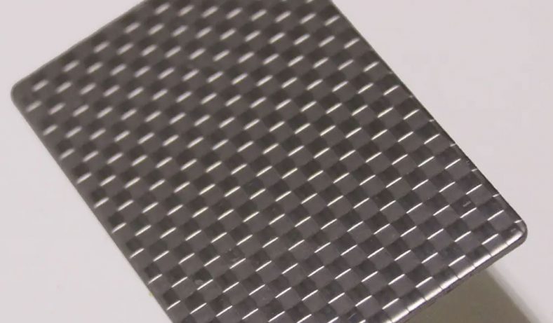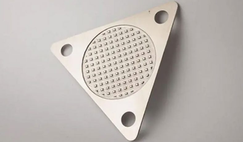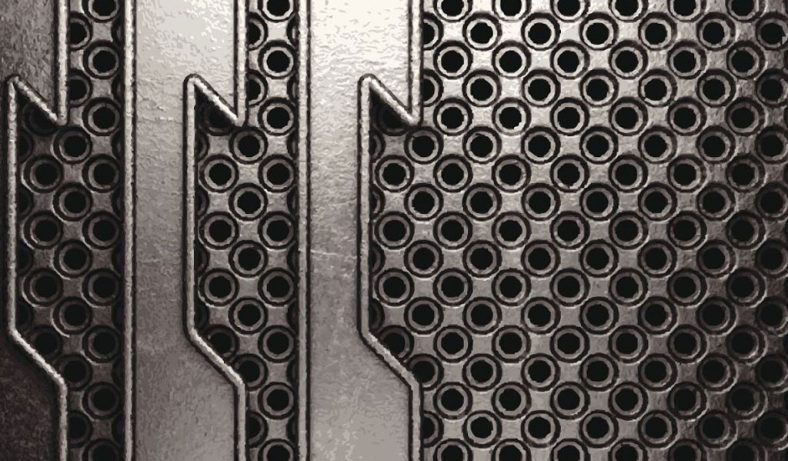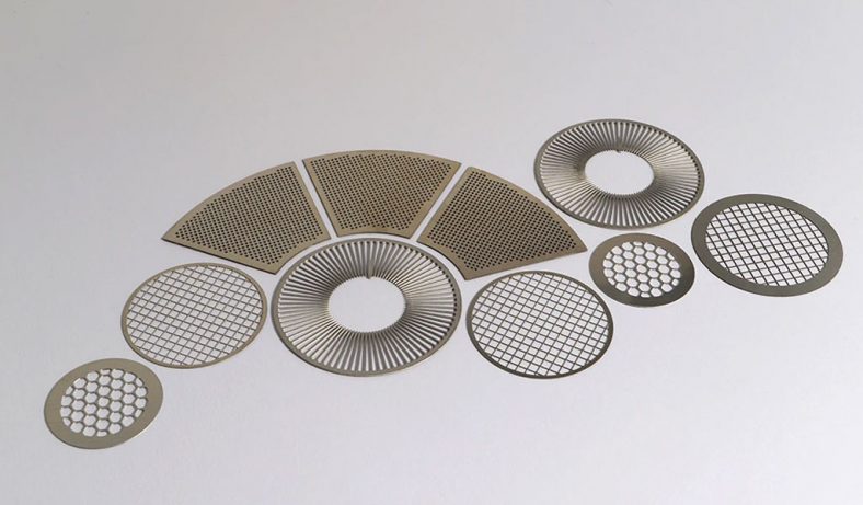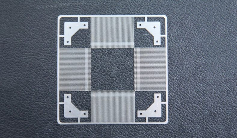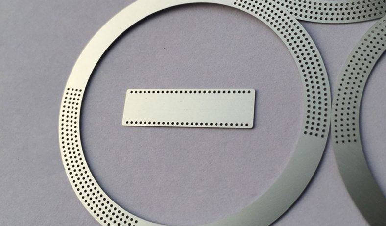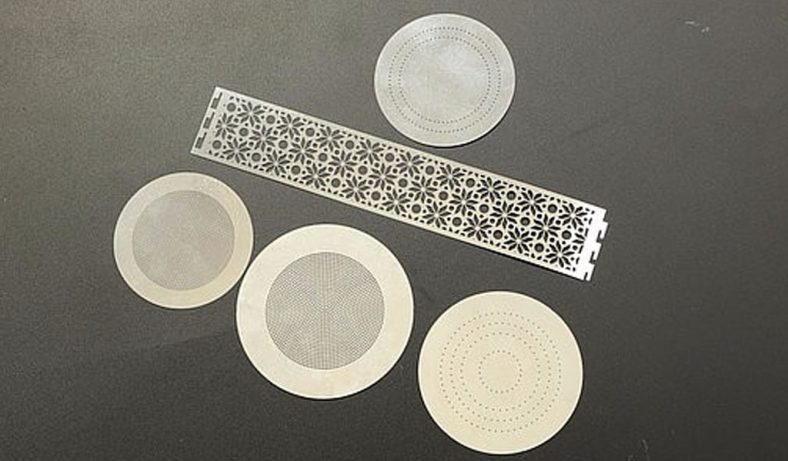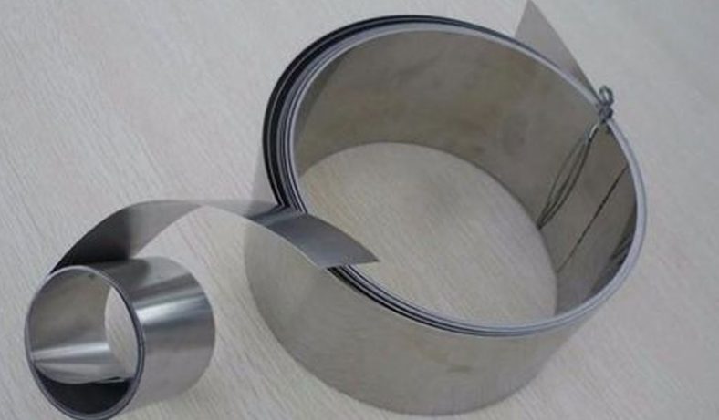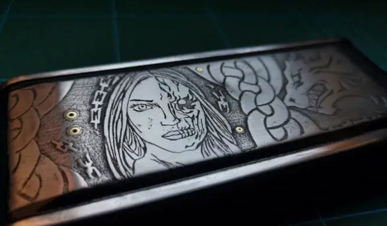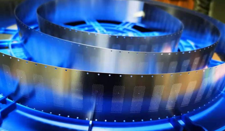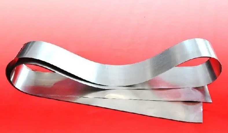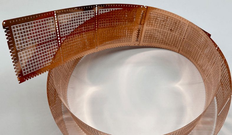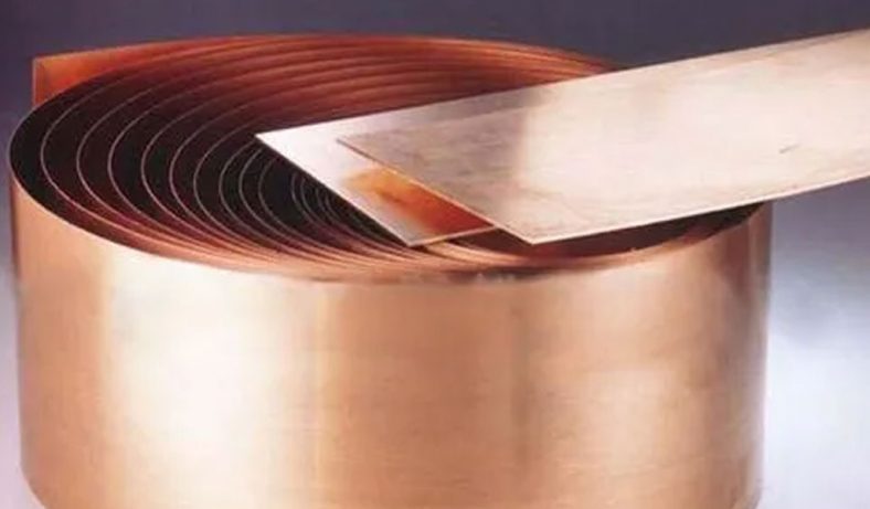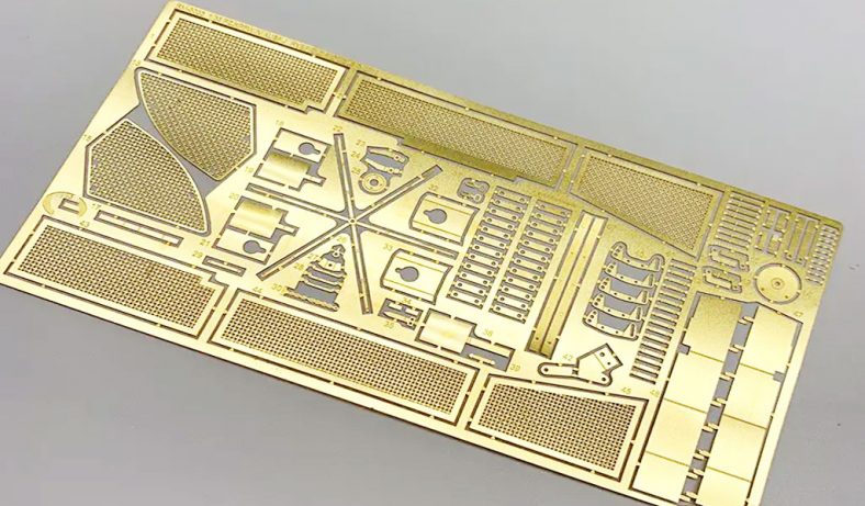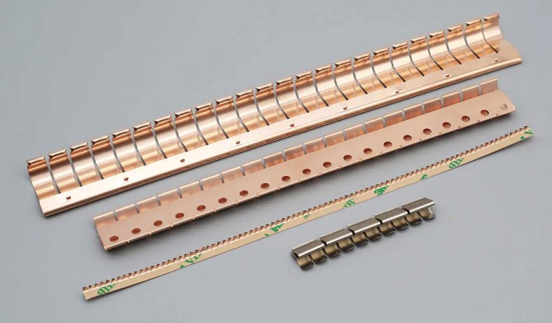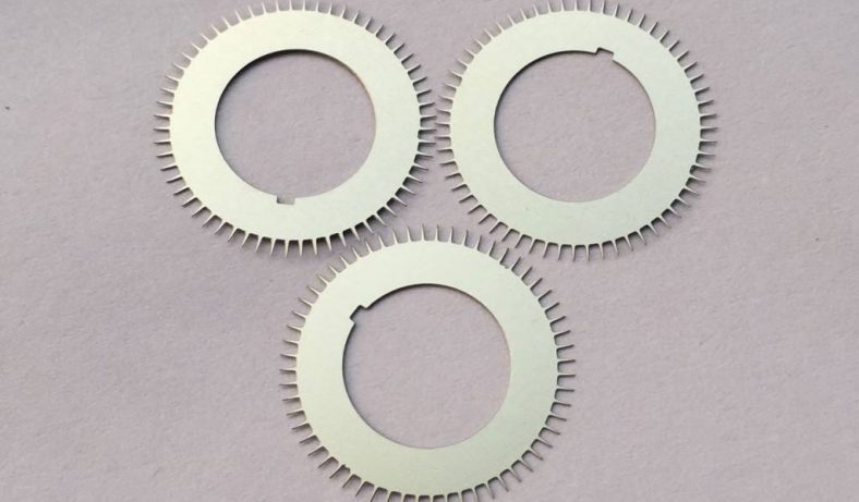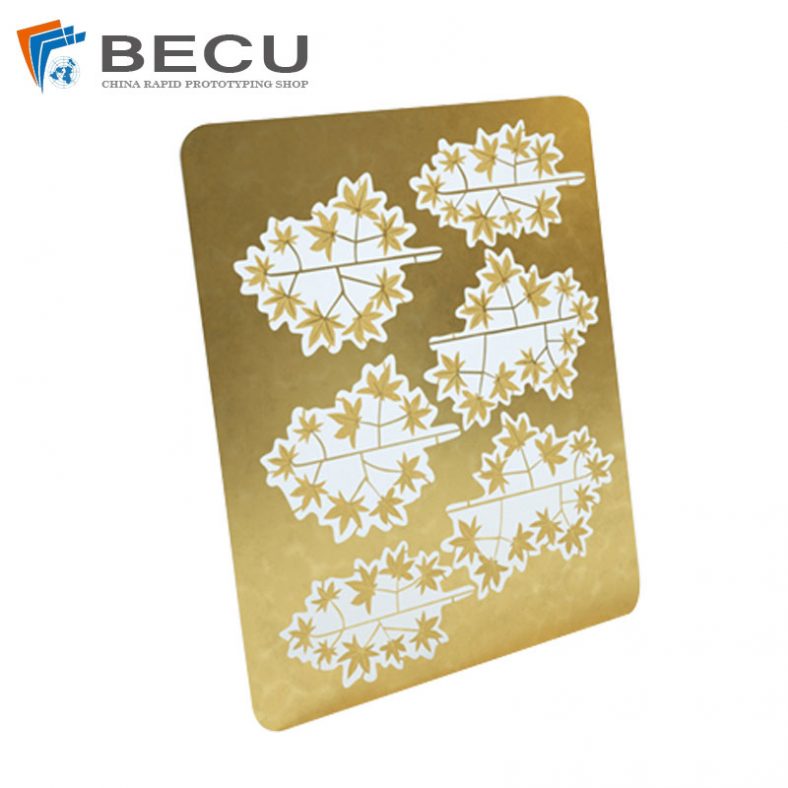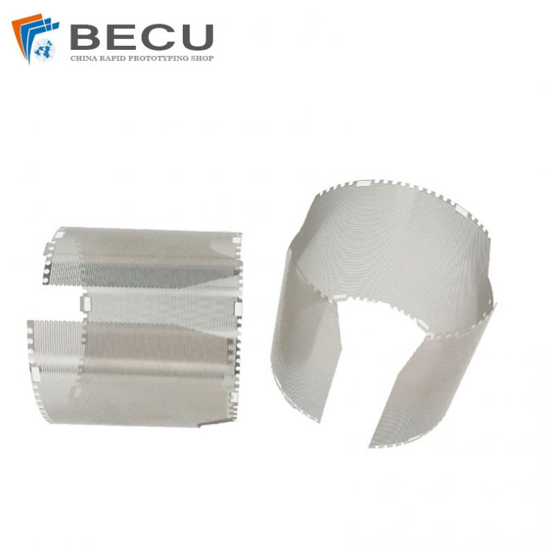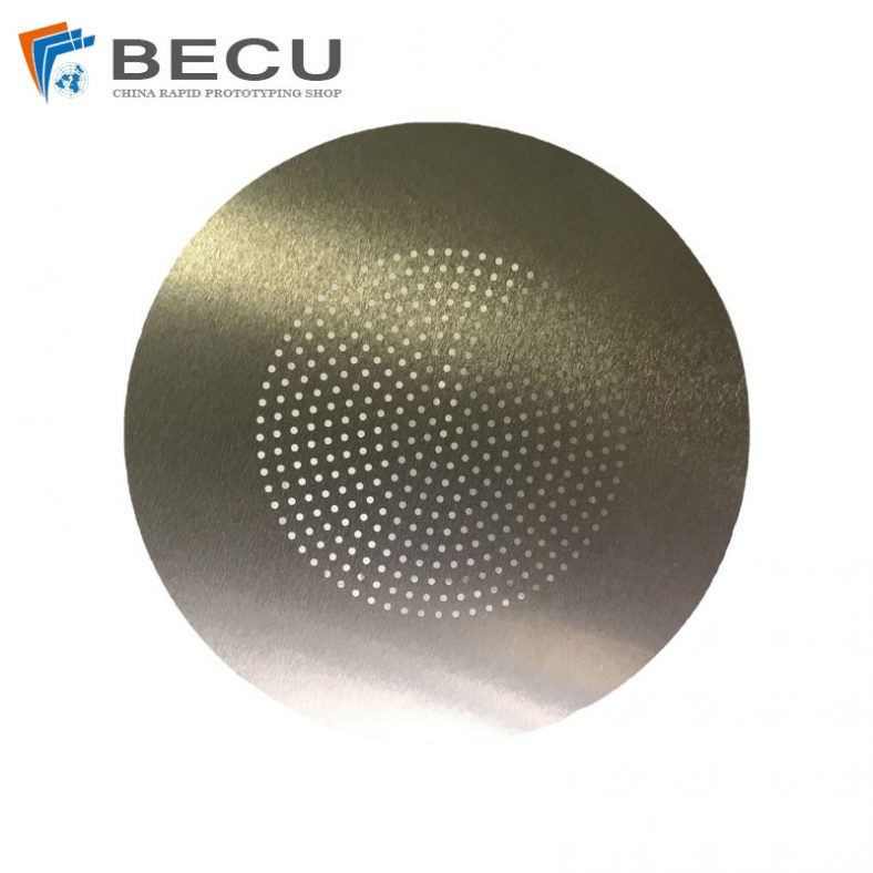
Metal etching is a critical manufacturing process in the semiconductor industry, enabling the precise fabrication of intricate components that are fundamental to modern electronic devices.
This process involves selectively removing material from a metal substrate to create the desired shapes, patterns, or features. Semiconductor manufacturing demands a high degree of precision, and metal etching fulfills this need by offering unparalleled accuracy, scalability, and reliability. Below, we explore the top 20 metal etching applications in the semiconductor sector, examining their roles, benefits, and contributions to advancing technology.
1. Photomask Production
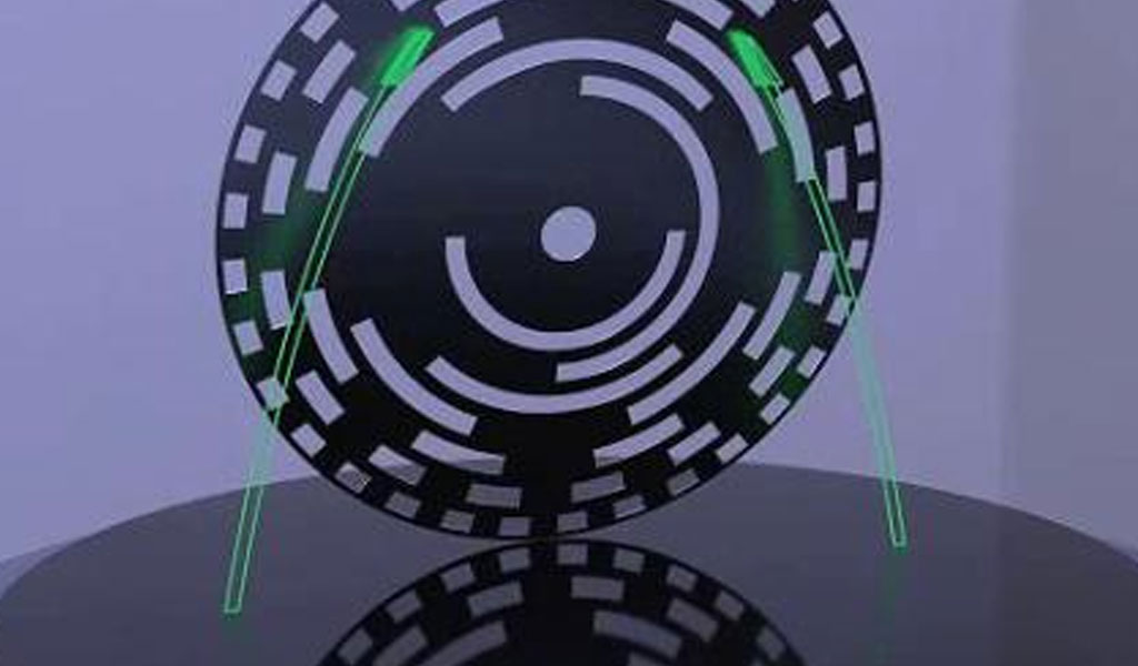
Photomasks are essential in the photolithography process, serving as a stencil for transferring patterns onto semiconductor wafers. Metal etching is used to create the ultra-precise patterns on these photomasks, often made of chrome-coated glass substrates. The precision of metal etching ensures that photomasks accurately define the intricate circuitry of integrated circuits (ICs).
2. Interconnects and Circuit Traces
Interconnects form the electrical pathways between components on a chip. Metal etching plays a crucial role in defining these pathways with exceptional accuracy. Copper and aluminum, commonly used as interconnect materials, undergo chemical or plasma etching to create narrow, high-aspect-ratio traces essential for advanced nodes in semiconductor manufacturing.
3. Lead Frames
Lead frames are metal structures used to connect semiconductor chips to external circuits. These components require tight tolerances and complex geometries, which are achieved through photo-chemical etching. This technique ensures that lead frames maintain consistent performance across large production volumes.
4. MEMS Devices
Micro-Electro-Mechanical Systems (MEMS) rely on etched metal components for their functionality. Metal etching is instrumental in fabricating tiny structures such as accelerometers, gyroscopes, and pressure sensors. Precision etching techniques enable the production of these microscale devices with the required accuracy and repeatability.
5. Shielding for EMI Protection
Electromagnetic interference (EMI) shielding is vital for protecting semiconductor devices from external electromagnetic signals. Etched metal shields are lightweight, compact, and highly effective in mitigating EMI. The process ensures the fine detail needed for perforated or slotted shield designs without compromising their performance.
6. Bond Pads
Bond pads are critical interfaces on semiconductor chips where electrical connections are made. Metal etching ensures the precise formation of these pads, which must meet stringent specifications to facilitate reliable wire bonding or flip-chip assembly. This accuracy is essential for the performance of modern microelectronic devices.
7. Power Semiconductor Components
Power semiconductors, such as MOSFETs and IGBTs, require robust and highly conductive metal layers for heat dissipation and current flow. Etching is used to define these metal layers, ensuring efficient operation. The process is critical in achieving the required thermal and electrical properties for power applications.
8. Thin-Film Resistors
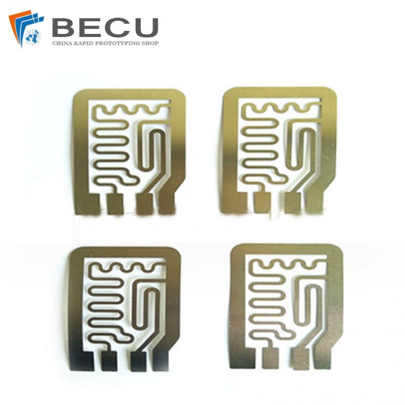
Metal etching is employed in the production of thin-film resistors, a key component in analog and mixed-signal ICs. The process allows for the precise adjustment of resistor values by carefully removing material, resulting in components with tight tolerances and excellent stability.
9. Packaging Substrates
Advanced semiconductor packaging often involves the use of metalized substrates to provide electrical connections and structural support. Etching is used to create complex patterns on these substrates, enabling the integration of multiple functions into compact packages such as system-in-package (SiP) and chip-on-board (CoB) assemblies.
10. Heat Spreaders
Heat spreaders are used to dissipate heat generated by high-performance semiconductor devices. Metal etching ensures the precise shaping and texturing of these components to maximize thermal performance. This is particularly important in applications like data centers, gaming, and high-frequency trading systems.
11. Sensor Components
Sensors for applications like IoT, automotive, and healthcare often require etched metal components. Examples include diaphragms, electrodes, and contact springs. Etching allows for the miniaturization and customization of these parts, enabling their integration into highly compact systems.
12. Antenna Structures
Wireless communication relies on highly efficient antenna designs. Metal etching is used to fabricate antennas with intricate patterns and precise dimensions, ensuring optimal signal transmission and reception. This is especially important in 5G and IoT applications, where performance is critical.
13. Capacitor and Inductor Elements
Capacitors and inductors in integrated circuits benefit from metal etching to define their electrode structures. Etching allows for the creation of fine features that improve component performance and enable their integration into densely packed semiconductor devices.
14. Power Distribution Networks
Efficient power distribution is crucial in semiconductor devices, particularly in high-performance computing and AI applications. Metal etching is used to create power planes and vias that ensure stable and reliable power delivery across the chip.
15. Microfluidic Devices
Metal etching is instrumental in the production of microfluidic devices used in labs-on-a-chip and biomedical applications. These devices often incorporate metal components such as electrodes, channels, and valves, all of which require the precision afforded by etching processes.
16. Optoelectronic Components
Optoelectronics, including LEDs, lasers, and photodetectors, rely on etched metal layers for electrical and thermal management. The precision of etching is critical to achieving the desired optical properties and ensuring the efficiency of these devices.
17. Signal Filters
Metal etching is used to fabricate signal filters, which are essential in RF and microwave communications. These components require intricate geometries to achieve specific frequency responses, and etching provides the necessary precision and consistency.
18. Test and Measurement Tools
Semiconductor testing relies on precise fixtures and tools, many of which incorporate etched metal components. Probes, sockets, and test boards all benefit from the accuracy and repeatability of metal etching, ensuring reliable and consistent testing results.
19. Die Attach Components
Die attach components, such as clips and plates, are etched to provide the required thermal and electrical properties for semiconductor devices. These components are critical in ensuring the mechanical stability and performance of chips in high-stress environments.
20. Flexible Circuits
Flexible circuits often integrate etched metal features to provide connectivity in compact and dynamic form factors. These circuits are widely used in wearables, medical devices, and other applications where space and flexibility are critical.
Conclusion
Metal etching has become an indispensable process in the semiconductor industry, enabling the production of components with exceptional precision, complexity, and reliability. Each application discussed highlights the versatility of metal etching in meeting the diverse and evolving demands of semiconductor manufacturing. As technology continues to advance, the role of metal etching will undoubtedly expand, driving innovations in electronics and beyond.

