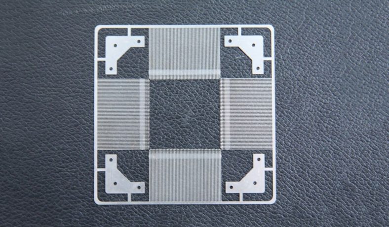
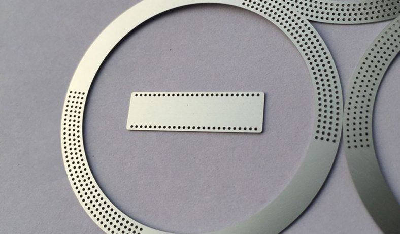
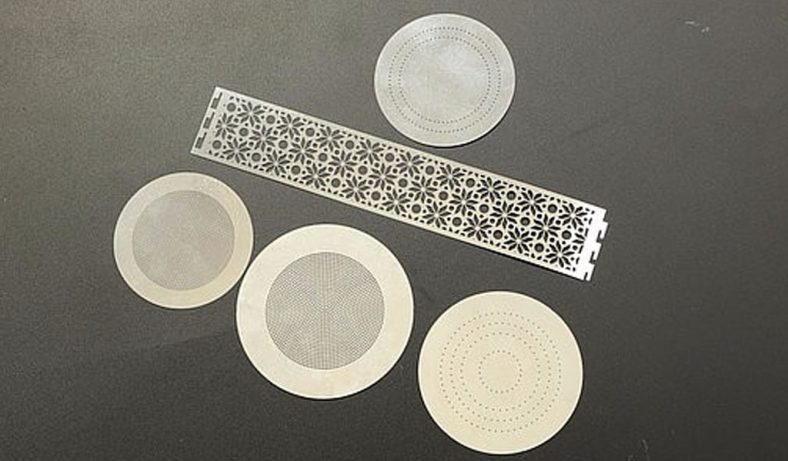
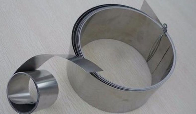
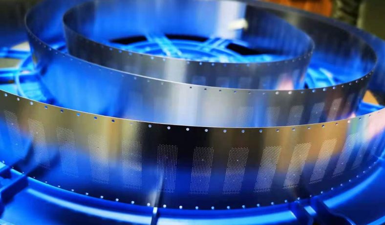
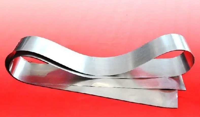
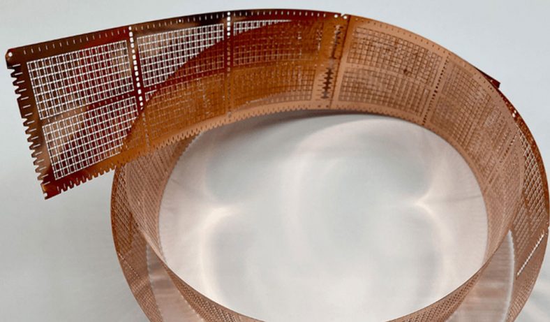
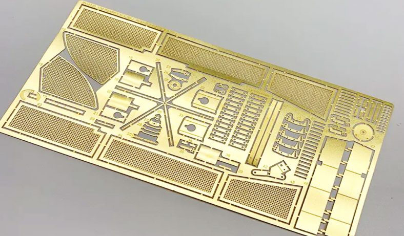
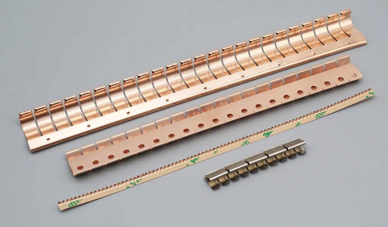
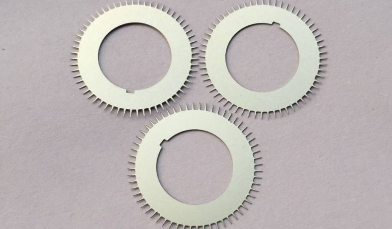
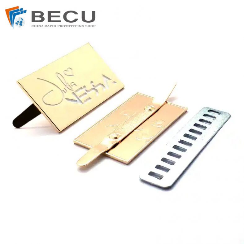
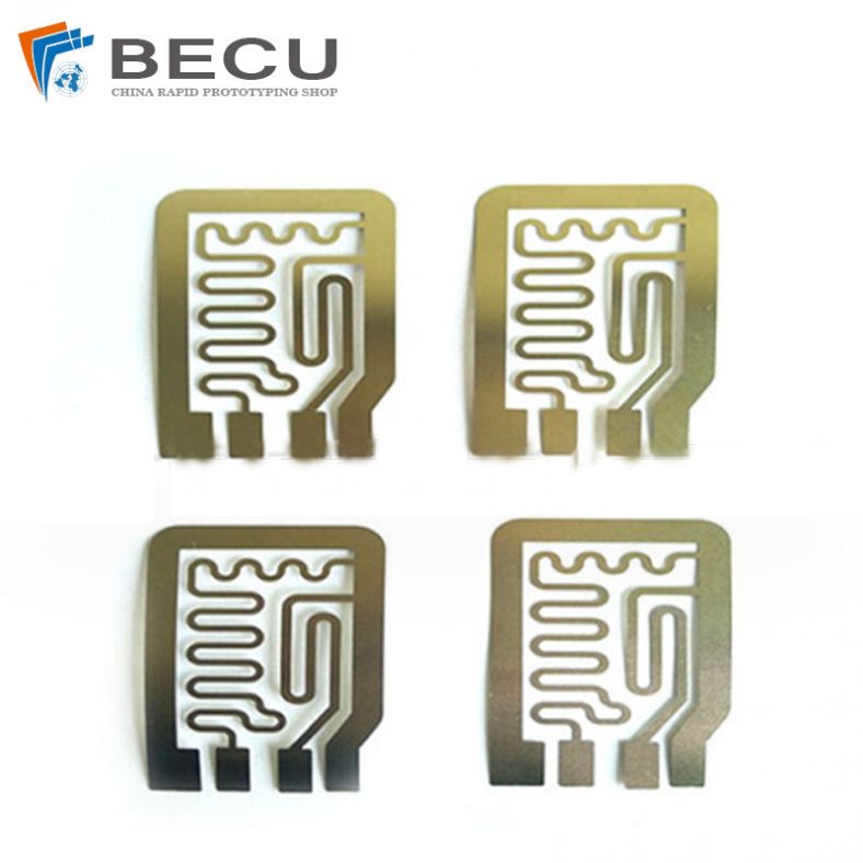
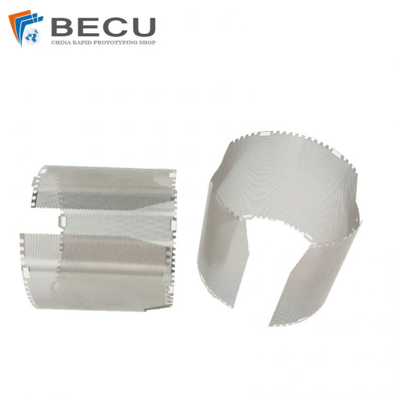
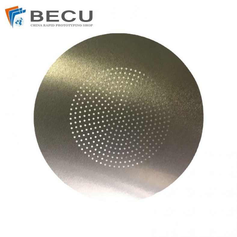
A leadframe is a crucial component in semiconductor packaging, serving as a metallic framework that provides electrical connections and mechanical support to semiconductor chips. Leadframes are essential in many electronic devices, acting as an intermediary between the microchip and the external circuitry. Their primary role is to carry electrical signals and power from the chip to external terminals while ensuring the structural stability of the package. This dual functionality has made leadframes indispensable in the electronics industry.
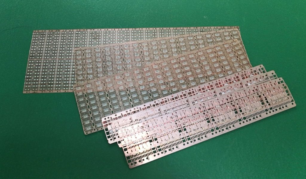
The Structure of a Leadframe
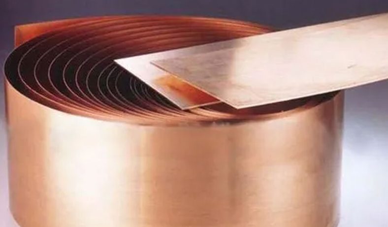
Leadframes typically consist of a thin sheet of metal, usually made from highly conductive materials like copper or copper alloys. Other materials, such as Alloy 42 (an iron-nickel alloy), are also used for specific applications requiring thermal expansion properties that match those of the silicon chip. The structure of a leadframe can vary widely depending on the type of semiconductor package it supports, including dual in-line packages (DIP), quad flat packages (QFP), and chip-on-board (COB) assemblies.
The metal sheet of a leadframe is precision-processed to form a network of leads, which are fine metallic strips extending from the chip’s bonding pads to the outer edge of the package. These leads allow for the transmission of electrical signals and power between the microchip and the external circuitry. The leads are connected to the chip via wire bonding, tape-automated bonding (TAB), or flip-chip bonding, depending on the design and requirements of the semiconductor device.
Manufacturing Processes for Leadframes
The production of leadframes involves a combination of materials science, mechanical engineering, and precision manufacturing techniques. Common methods include stamping, etching, and plating.
- Stamping: Stamping is one of the most common methods for producing leadframes in high volumes. This process involves feeding a metal strip through a stamping press equipped with a die that cuts and forms the metal into the desired leadframe pattern. Stamping is cost-effective for large-scale production but may have limitations in achieving extremely fine geometries.
- Chemical Etching: Etching is a photolithography-based process that allows for the creation of intricate patterns with high precision. In this method, a photoresist is applied to the metal sheet, and the desired leadframe design is transferred using ultraviolet light. The exposed areas are then chemically etched away, leaving behind the leadframe pattern. Chemical etching is particularly useful for complex designs or prototypes.
- Plating: After the leadframe is formed, it is often plated with materials like gold, silver, palladium, or tin to improve its electrical conductivity, corrosion resistance, and bonding properties. Plating can be selective or full-surface, depending on the application.
- Assembly and Testing: Once the leadframe is manufactured, it undergoes further processing, including chip attachment, wire bonding, encapsulation, and testing to ensure its functionality and reliability.
The Role of Leadframes in Semiconductor Packaging
Leadframes are fundamental to semiconductor packaging, which protects microchips from environmental damage while enabling electrical connectivity. Packaging ensures that the delicate microchip can be integrated into electronic devices and operate reliably over its lifetime.Key Functions of Leadframes:
- Electrical Connection: Leadframes provide a pathway for electrical signals and power between the microchip and external circuitry. The quality and design of the leads significantly impact the electrical performance of the device.
- Thermal Management: Many leadframes include features like heat slugs or thermal pads to dissipate heat generated by the chip during operation, ensuring stable performance and longevity.
- Mechanical Support: The leadframe provides structural integrity to the package, holding the chip in place and maintaining the alignment of the leads for reliable connectivity.
- Cost Efficiency: Leadframes are a cost-effective solution for high-volume semiconductor manufacturing, making them a popular choice for a wide range of applications.
Metal Etching in Leadframe Manufacturing
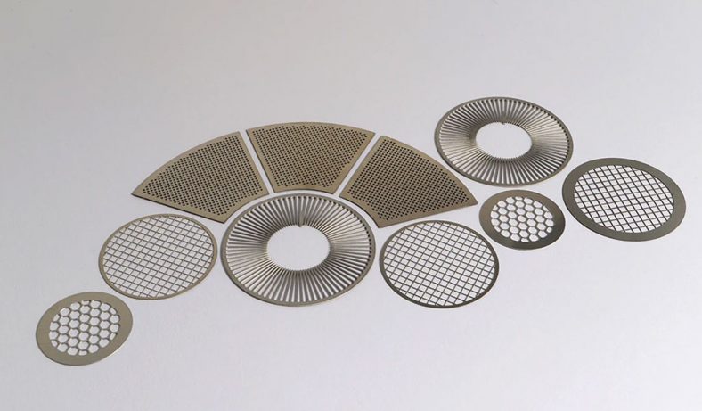
Metal etching has emerged as a key technology in leadframe manufacturing, particularly for applications requiring precision and intricate designs. This process, also known as chemical milling or photo-chemical machining, allows manufacturers to produce highly detailed and consistent leadframe patterns with minimal material wastage.
Process of Metal Etching:
- Material Preparation: A sheet of metal, typically copper or copper alloy, is selected based on the desired properties of the leadframe. The metal sheet is cleaned to remove contaminants that could interfere with the etching process.
- Photoresist Application: A photoresist material is applied to the metal sheet. This light-sensitive coating will define the areas to be etched and protected.
- Image Transfer: The leadframe design is transferred onto the photoresist-coated metal sheet using ultraviolet light. A photomask, which contains the desired leadframe pattern, ensures precise exposure.
- Development: The photoresist is developed, revealing the metal areas to be etched while protecting the rest.
- Chemical Etching: The metal sheet is exposed to a chemical etchant, such as ferric chloride or cupric chloride, which dissolves the unprotected areas. The result is a highly precise leadframe pattern.
- Stripping and Finishing: After etching, the remaining photoresist is stripped away, and the leadframe undergoes additional processes like plating, cleaning, and inspection to ensure quality.
Advantages of Metal Etching:
- Precision: Etching can achieve extremely fine geometries, making it ideal for modern semiconductor devices with tight tolerances.
- Flexibility: The process can easily accommodate design changes and complex patterns without the need for new tooling.
- Cost-Effectiveness: For low to medium production volumes or highly detailed designs, etching is often more economical than stamping.
- Material Integrity: Unlike stamping, which can introduce stress and deformation, etching preserves the material’s structural properties.
Applications of Metal-Etched Leadframes
Metal-etched leadframes are used across various industries and applications, reflecting their versatility and precision. Common areas of application include:
- Consumer Electronics: Leadframes are integral to devices like smartphones, tablets, and wearable technology, ensuring reliable performance in compact designs.
- Automotive Electronics: In vehicles, leadframes are used in engine control units (ECUs), sensors, and lighting systems, where precision and durability are critical.
- Medical Devices: Semiconductor packages with etched leadframes are employed in medical equipment such as pacemakers, imaging devices, and diagnostic tools.
- Industrial Automation: Leadframes support components in robotics, control systems, and other industrial automation technologies.
- Aerospace and Defense: High-reliability leadframes are used in aerospace and defense applications, where performance under extreme conditions is essential.
Innovations in Leadframe and Etching Technologies
Advancements in materials science, etching techniques, and semiconductor packaging have driven innovations in leadframe manufacturing. Key trends include:
- Miniaturization: As electronic devices become smaller and more powerful, leadframes must accommodate finer geometries and higher pin counts.
- Material Optimization: Researchers are exploring new materials and alloys to improve leadframe performance in terms of thermal management, electrical conductivity, and environmental resistance.
- Advanced Plating Techniques: Innovations in selective and multi-layer plating enhance the functionality and reliability of leadframes.
- Sustainability: Eco-friendly etching solutions and recycling of etchant chemicals are being developed to reduce the environmental impact of leadframe production.
Conclusion
Leadframes and metal etching are at the heart of modern semiconductor manufacturing, providing the precision, functionality, and reliability needed for electronic devices. As technology continues to evolve, leadframe production will remain a dynamic and innovative field, ensuring its central role in the electronics industry. Through advanced etching techniques and material innovations, the capabilities of leadframes will continue to expand, meeting the demands of next-generation applications.

