
Trend
The etching process is a fundamental technique in materials science, semiconductor manufacturing, and various industrial applications, where controlled ...

Wet etching is a cornerstone technique in microfabrication, particularly for processing aluminum alloys in the production of micro-devices, such as ...

Photolithography and etching are cornerstone processes in the field of micromachining, particularly when applied to materials such as stainless steel, which ...

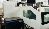
Metal etching, a critical process in manufacturing industries such as electronics, aerospace, and energy, involves the selective removal of material from ...
Wet etching is a cornerstone of microfabrication, particularly in the production of micro-devices where precision, repeatability, and material integrity are ...

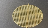
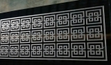
Electromagnetic interference (EMI) shielding is a critical aspect of modern electronics, ensuring that sensitive components are protected from unwanted ...
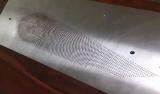
Aluminum etching technology has emerged as a pivotal manufacturing process in the production of precision components for medical devices, particularly ...
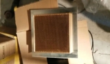
Electromagnetic interference (EMI) and radio frequency interference (RFI) pose significant challenges to the performance of modern electronic systems, ...
Twisted bilayer graphene (TBG) has emerged as a transformative platform in condensed matter physics and materials science due to its unique electronic, ...

Molybdenum disulfide (MoS₂), a two-dimensional (2D) transition metal dichalcogenide (TMD), has emerged as a cornerstone material in the rapidly evolving field ...

Sapphire, a crystalline form of aluminum oxide (Al₂O₃), is a cornerstone material in the fabrication of gallium nitride (GaN)-based light-emitting diodes ...
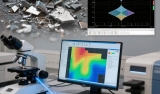
Virtual metrology (VM) is an advanced methodology employed in semiconductor manufacturing to predict critical process outcomes, such as etch rates, feature ...

Wet etching is a critical process in the fabrication of compound semiconductor devices, enabling precise patterning and surface modification essential for ...
Silicon carbide (SiC) is a wide-bandgap semiconductor material renowned for its exceptional physical and chemical properties, including high thermal ...
Two-dimensional (2D) materials, such as graphene, transition metal dichalcogenides (TMDs), and hexagonal boron nitride (hBN), have emerged as pivotal ...

High-selectivity plasma etching is a critical process in the fabrication of advanced Fin Field-Effect Transistor (FinFET) structures, enabling the precise ...

Gallium nitride (GaN) is a wide-bandgap semiconductor material that has garnered significant attention in the field of power electronics due to its ...
Micro-Electro-Mechanical Systems (MEMS) represent a transformative technology that integrates mechanical and electrical components at the microscale, enabling ...

Atomic Layer Etching (ALE) is a cutting-edge nanofabrication technique that enables the precise removal of material at the atomic scale, offering unparalleled ...

Anisotropic wet etching of sapphire substrates is a critical process in the fabrication of high-performance light-emitting diodes (LEDs), particularly those ...
