
Virtual metrology (VM) is an advanced methodology employed in semiconductor manufacturing to predict critical process outcomes, such as etch rates, feature ...
Wet etching is a critical process in the fabrication of compound semiconductor devices, enabling precise patterning and surface modification essential for ...
Silicon carbide (SiC) is a wide-bandgap semiconductor material renowned for its exceptional physical and chemical properties, including high thermal ...
Two-dimensional (2D) materials, such as graphene, transition metal dichalcogenides (TMDs), and hexagonal boron nitride (hBN), have emerged as pivotal ...

High-selectivity plasma etching is a critical process in the fabrication of advanced Fin Field-Effect Transistor (FinFET) structures, enabling the precise ...
Gallium nitride (GaN) is a wide-bandgap semiconductor material that has garnered significant attention in the field of power electronics due to its ...
Micro-Electro-Mechanical Systems (MEMS) represent a transformative technology that integrates mechanical and electrical components at the microscale, enabling ...

Atomic Layer Etching (ALE) is a cutting-edge nanofabrication technique that enables the precise removal of material at the atomic scale, offering unparalleled ...

Anisotropic wet etching of sapphire substrates is a critical process in the fabrication of high-performance light-emitting diodes (LEDs), particularly those ...
Dry etching is a cornerstone of modern semiconductor fabrication, enabling the precise patterning of materials at nanometer scales. As the semiconductor ...

Inductively Coupled Plasma (ICP) etching is a cornerstone technology in the fabrication of micro and nanoscale devices, particularly for silicon-based ...
The semiconductor industry has been a cornerstone of technological advancement, enabling the development of integrated circuits (ICs) that power modern ...
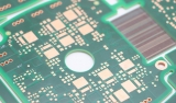
High aspect ratio (HAR) plasma etching is a cornerstone of modern semiconductor device fabrication, enabling the creation of intricate nanoscale features ...

Deep Reactive Ion Etching (DRIE) is a highly anisotropic plasma etching process used to create deep, steep-sided holes and trenches in substrates, typically ...
Reactive Ion Etching (RIE) is a cornerstone technology in microfabrication, pivotal for the precise structuring of materials at the micro- and nanoscale. ...

High-density plasma (HDP) etching systems are pivotal in the semiconductor industry, enabling the fabrication of intricate micro- and nanoscale features ...

Metal etching is a critical manufacturing process used to selectively remove material from metal surfaces to create intricate patterns, microstructures, or ...
Photoresist stripping is a critical step in the photochemical etching process, a subtractive manufacturing technique used to create precise, intricate metal ...

Plasma etching is a cornerstone technology in micro- and nanofabrication, enabling precise pattern transfer in the production of advanced electronic, optical, ...
Magnesium alloys, characterized by their low density, high strength-to-weight ratio, and biocompatibility, have emerged as promising materials for ...
- « Previous Page
- 1
- 2
- 3
- 4
- …
- 10
- Next Page »