Lithium-ion batteries (LIBs) have become the cornerstone of modern energy storage solutions, powering a wide array of devices from portable electronics to electric vehicles. The quest for higher energy densities and improved performance has led researchers to explore novel materials and architectures for battery electrodes. Among the various candidates, silicon (Si) has emerged as a promising anode material due to its high theoretical capacity, which is approximately ten times that of conventional graphite anodes. However, the practical implementation of silicon anodes is hindered by significant volume changes during lithiation and delithiation, leading to mechanical degradation and capacity fading.
One innovative approach to mitigate these issues is the preparation of nanosilicon wires (NSWs) through chemical etching. This method allows for the creation of nanostructured silicon with enhanced mechanical stability and electrochemical performance. This article delves into the intricacies of preparing nanosilicon wires by chemical etching, their application as negative electrodes in high-energy lithium-ion batteries, and a comprehensive comparison with other anode materials.
Chemical Etching of Silicon
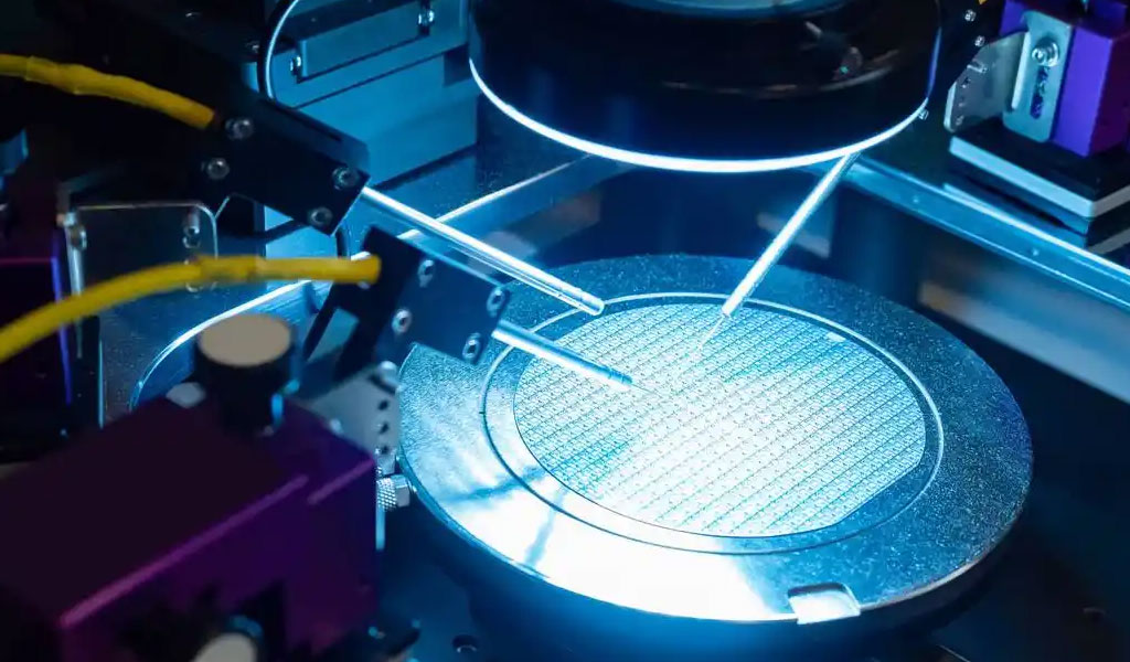
Chemical etching is a well-established technique in semiconductor manufacturing, used to selectively remove material from a substrate. In the context of preparing nanosilicon wires, chemical etching involves the use of specific etchants that can create nanoscale structures on silicon wafers. The most commonly used etchant for this purpose is a mixture of hydrofluoric acid (HF) and silver nitrate (AgNO₃).
Mechanism of Chemical Etching
The chemical etching process for silicon involves several steps:
- Oxidation: The silicon surface is first oxidized to form a thin layer of silicon dioxide (SiO₂). This can be achieved through thermal oxidation or by exposing the silicon to an oxidizing agent.
- Etching: The oxidized silicon is then exposed to an etchant solution, typically a mixture of HF and AgNO₃. The HF etches the SiO₂ layer, while the AgNO₃ acts as a catalyst to facilitate the etching process.
- Nanostructure Formation: As the etching progresses, nanoscale pores or wires are formed on the silicon surface. The morphology of these nanostructures can be controlled by adjusting the concentration of the etchant, the etching time, and other process parameters.
Factors Affecting Chemical Etching
Several factors influence the outcome of the chemical etching process:
- Etchant Concentration: The concentration of HF and AgNO₃ in the etchant solution plays a crucial role in determining the etching rate and the morphology of the resulting nanostructures. Higher concentrations generally lead to faster etching rates and more pronounced nanostructures.
- Etching Time: The duration of the etching process affects the depth and uniformity of the nanostructures. Prolonged etching can result in deeper pores or wires but may also lead to increased surface roughness.
- Temperature: The temperature at which the etching process is conducted can influence the etching rate and the quality of the nanostructures. Higher temperatures typically accelerate the etching process but may also introduce thermal stresses in the silicon substrate.
- Silicon Substrate: The type and quality of the silicon substrate can affect the etching process. Single-crystal silicon wafers are preferred due to their uniformity and high purity, which ensure consistent etching results.
Preparation of Nanosilicon Wires
The preparation of nanosilicon wires involves a series of steps, including substrate preparation, chemical etching, and post-etching treatments.
Substrate Preparation
The first step in preparing nanosilicon wires is the selection and preparation of the silicon substrate. High-purity, single-crystal silicon wafers are commonly used due to their uniformity and consistency. The wafers are typically cleaned using standard semiconductor cleaning procedures, such as the RCA clean, to remove any surface contaminants.
Chemical Etching Process
The cleaned silicon wafers are then subjected to the chemical etching process. The etchant solution, typically a mixture of HF and AgNO₃, is prepared with precise concentrations to achieve the desired etching rate and nanostructure morphology. The wafers are immersed in the etchant solution for a controlled period, during which the etching process occurs.
Post-Etching Treatments
After the etching process, the silicon wafers are rinsed thoroughly to remove any residual etchant and reaction byproducts. Additional post-etching treatments, such as thermal annealing or surface passivation, may be performed to enhance the mechanical stability and electrochemical performance of the nanosilicon wires.
Characterization of Nanosilicon Wires
The characterization of nanosilicon wires is essential to understand their structural, mechanical, and electrochemical properties. Various analytical techniques are employed for this purpose:
- Scanning Electron Microscopy (SEM): SEM is used to visualize the morphology and dimensions of the nanosilicon wires. High-resolution SEM images provide detailed information about the wire diameter, length, and surface roughness.
- Transmission Electron Microscopy (TEM): TEM offers higher resolution imaging compared to SEM and is used to study the internal structure and crystallinity of the nanosilicon wires.
- X-ray Diffraction (XRD): XRD is employed to analyze the crystallographic structure of the nanosilicon wires. The diffraction patterns provide insights into the crystal orientation and any structural defects.
- Raman Spectroscopy: Raman spectroscopy is used to study the vibrational modes of the nanosilicon wires, providing information about their chemical composition and bonding characteristics.
- Electrochemical Testing: The electrochemical performance of the nanosilicon wires is evaluated using techniques such as cyclic voltammetry (CV), galvanostatic charge-discharge (GCD), and electrochemical impedance spectroscopy (EIS). These tests assess the capacity, rate capability, and cycling stability of the nanosilicon wires as anode materials in lithium-ion batteries.
Application in Lithium-Ion Batteries
Nanosilicon wires hold great promise as negative electrodes in high-energy lithium-ion batteries due to their unique properties:
- High Theoretical Capacity: Silicon has a theoretical capacity of approximately 4200 mAh/g, which is significantly higher than that of graphite (372 mAh/g). This high capacity makes silicon an attractive candidate for high-energy batteries.
- Enhanced Mechanical Stability: The nanostructured morphology of nanosilicon wires provides improved mechanical stability compared to bulk silicon. The nanowires can accommodate the volume changes during lithiation and delithiation, reducing the risk of mechanical degradation and capacity fading.
- Improved Electrochemical Performance: The large surface area and short diffusion paths in nanosilicon wires enhance their electrochemical performance. The nanowires exhibit high rate capability and improved cycling stability, making them suitable for high-power applications.
Comparison with Other Anode Materials
To understand the advantages and limitations of nanosilicon wires as anode materials, it is essential to compare them with other commonly used anode materials. The following table provides a detailed comparison:
| Property | Graphite | Silicon | Lithium Titanate (LTO) | Tin (Sn) | Nanosilicon Wires |
|---|---|---|---|---|---|
| Theoretical Capacity | 372 mAh/g | 4200 mAh/g | 175 mAh/g | 994 mAh/g | 4200 mAh/g |
| Volumetric Capacity | 837 mAh/cm³ | 2360 mAh/cm³ | 610 mAh/cm³ | 2091 mAh/cm³ | 2360 mAh/cm³ |
| Operating Voltage | 0.1-0.2 V vs. Li/Li⁺ | 0.1-0.5 V vs. Li/Li⁺ | 1.55 V vs. Li/Li⁺ | 0.4-0.6 V vs. Li/Li⁺ | 0.1-0.5 V vs. Li/Li⁺ |
| Volume Change | ~10% | ~300% | ~1% | ~260% | ~300% |
| Mechanical Stability | High | Low | High | Low | High |
| Rate Capability | Moderate | High | High | Moderate | High |
| Cycling Stability | High | Low | High | Low | High |
| Cost | Low | Moderate | High | Moderate | Moderate |
| Safety | Moderate | Moderate | High | Moderate | Moderate |
Graphite
Graphite is the most commonly used anode material in commercial lithium-ion batteries due to its low cost, high stability, and well-established manufacturing processes. However, its relatively low theoretical capacity limits its application in high-energy batteries.
Silicon
Bulk silicon offers a high theoretical capacity but suffers from significant volume changes during lithiation and delithiation, leading to mechanical degradation and poor cycling stability. Nanosilicon wires address these issues by providing enhanced mechanical stability and improved electrochemical performance.
Lithium Titanate (LTO)
Lithium titanate (LTO) is known for its high safety and excellent cycling stability. However, its low theoretical capacity and high operating voltage limit its application in high-energy batteries.
Tin (Sn)
Tin is another high-capacity anode material with a theoretical capacity of 994 mAh/g. However, it also experiences significant volume changes during lithiation and delithiation, leading to mechanical degradation and poor cycling stability.
Challenges and Future Directions
While nanosilicon wires hold great promise as anode materials for high-energy lithium-ion batteries, several challenges need to be addressed:
- Volume Changes: Although nanosilicon wires offer improved mechanical stability compared to bulk silicon, the significant volume changes during lithiation and delithiation remain a challenge. Further research is needed to develop strategies to mitigate these volume changes and enhance the cycling stability of nanosilicon wires.
- Surface Passivation: The large surface area of nanosilicon wires makes them susceptible to side reactions with the electrolyte, leading to the formation of a solid electrolyte interphase (SEI) layer. Optimizing the surface passivation of nanosilicon wires is crucial to minimize these side reactions and improve their electrochemical performance.
- Scalability: The preparation of nanosilicon wires by chemical etching is currently a laboratory-scale process. Scaling up this process for commercial production is a significant challenge that requires innovative manufacturing techniques and process optimization.
- Cost: The cost of producing nanosilicon wires is currently higher than that of conventional graphite anodes. Reducing the production cost through process optimization and economies of scale is essential for the widespread adoption of nanosilicon wires in commercial lithium-ion batteries.
Conclusion
The preparation of nanosilicon wires by chemical etching offers a promising approach to developing high-energy lithium-ion batteries. The nanostructured morphology of nanosilicon wires provides enhanced mechanical stability and improved electrochemical performance, making them suitable for high-power applications. However, several challenges, including volume changes, surface passivation, scalability, and cost, need to be addressed to realize the full potential of nanosilicon wires as anode materials.
Continued research and development in this field are essential to overcome these challenges and pave the way for the commercialization of nanosilicon wires in high-energy lithium-ion batteries. The successful implementation of nanosilicon wires as anode materials could revolutionize the energy storage industry, enabling the development of batteries with higher energy densities, improved performance, and enhanced safety.

