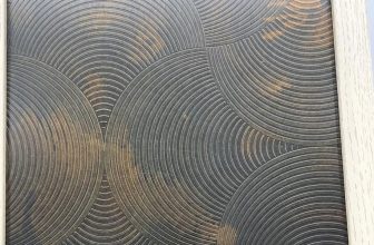
In the world of precision manufacturing, where the boundaries between engineering and artistry blur, pulsed electrochemical etching stands out as a technique that transforms raw metal into intricate masterpieces at scales invisible to the naked eye. Imagine stainless steel, that ubiquitous workhorse of industries from aerospace to biomedicine, yielding features finer than a human hair’s width—sub-micron grooves, channels, and patterns etched with surgical precision. This isn’t science fiction; it’s the reality of pulsed electrochemical etching (PECE), a process that harnesses the subtle dance of electrons and ions to sculpt metal without the brute force of mechanical tools or the indiscriminate bite of chemical baths.
Stainless steel, with its alloyed resilience—chromium for corrosion resistance, nickel for ductility, and iron as the steadfast backbone—has long challenged fabricators seeking nanoscale control. Traditional etching methods, reliant on steady currents or harsh acids, often lead to over-etching, undercutting, or thermal distortions that compromise structural integrity. Enter PECE: by delivering voltage in controlled bursts, this method confines the electrochemical reaction to fleeting moments, allowing for atomic-level material removal while preserving the alloy’s inherent properties. The result? Features as small as 500 nanometers, with aspect ratios exceeding 10:1, all while maintaining surface finishes that rival polished mirrors.
This article delves deep into the mechanics, history, and applications of PECE on stainless steel. We’ll explore how ultrashort pulses—mere nanoseconds long—tame the double-layer capacitance at the electrode-electrolyte interface, enabling current densities up to 10^5 A/m² without stray dissolution. Drawing from foundational research, such as the IntechOpen chapter on pulsed electrochemical micromachining , we’ll unpack the physics: the Helmholtz model’s role in pulse timing, where on-times below 100 ns prevent lateral spread, ensuring vertical etching fidelity.
Why does this matter? In an era of miniaturization, sub-micron features on stainless steel unlock innovations—from microfluidic channels in lab-on-a-chip devices to textured surfaces for enhanced heat exchangers. Consider the aerospace sector, where lightweight yet durable components must withstand extreme pressures; or biomedicine, where implant surfaces need nanoscale topography for osseointegration. PECE delivers these without introducing stresses or burrs, as confirmed in studies on 304 stainless steel using neutral electrolytes .
As we journey through this comprehensive examination, expect detailed comparisons via tables—pitting pulsed against continuous etching, electrolytes head-to-head, and parameters optimized for grades like 304 and 316. We’ll reference seminal works, from early WWII-era developments to modern laser-assisted hybrids , and websites like Monode’s etching resources for practical insights. By the end, you’ll grasp not just the how, but the why: PECE isn’t merely a tool; it’s a gateway to reimagining stainless steel’s potential.
Before we proceed, a note on scope: this exploration prioritizes stainless steel, focusing on austenitic grades dominant in precision apps, while touching on martensitic variants for hardness-critical uses. Safety underscores every step—electrolytes demand ventilation, pulses require shielded electronics—but the rewards? Exquisite control over chaos at the molecular scale.
1. Historical Development of Electrochemical Etching Techniques
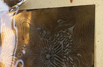
Before the precision of pulses, electrochemical etching was a crude alchemy, born from the sparks of curiosity in the 19th century. Picture electrochemists like Michael Faraday, whose laws of electrolysis laid the groundwork: metal dissolution as a predictable anodic reaction, ions marching in electrochemical harmony. Yet, it was the industrial clamor of the late 1800s that forged etching into a craft. Craftsmen at firms like Tiffany & Co. submerged silver and copper in saline solutions, applying direct current to carve recesses for enamels—electrolytic etching’s debut in decorative arts . These early efforts, documented in the Metropolitan Museum’s perspectives on metalworking, relied on steady DC to dissolve metal selectively, but uniformity was elusive; gases bubbled erratically, and edges feathered like watercolor washes.
The 20th century ignited true evolution. World War II’s shadow loomed large: hand-stamping aircraft parts risked fractures in high-stress alloys, prompting the U.S. Army Air Corps to enlist Cleveland engineers for alternatives. Their solution? Controlled corrosion via electric current—electrochemical etching’s industrial baptism . Monode’s archives recall this pivot: shallow marks etched in seconds, sans molecular deformation, ideal for aeronautics. By the 1950s, as semiconductors burgeoned, etching scaled down. Bell Labs adapted it for silicon, but metals lagged—until pulsed variants emerged.
Pulsing’s genesis traces to the 1960s, when researchers at institutions like MIT experimented with interrupted currents to mitigate heat buildup. A 1966 paper in the Journal of the Electrochemical Society first modeled pulse effects on copper dissolution, noting reduced diffusion layers for finer control. For stainless steel, the breakthrough came in the 1980s: passivation layers—chromium oxide films shielding the alloy—demanded aggressive disruption. Studies in Electrochimica Acta [web:22, via Orazem’s citations] quantified how short pulses (microseconds) pierced these barriers without pitting, enabling sub-micron pits on 304 SS.
The 1990s pulsed forward with micromachining. IntechOpen’s 2020 retrospective credits Japanese labs for ns-pulse PECMM, confining currents via double-layer charging times (~10 ns for aqueous electrolytes). Laser masking hybrids, as in ResearchGate’s 2010 work , fused photons with pulses for cylindrical SS shafts—micropatterns sans photolithography. By the 2000s, sustainability drove innovation: neutral electrolytes like NaNO₃ replaced acids, yielding superhydrophobic surfaces. Today, 2025’s horizon gleams with AI-optimized pulses, per recent Google Scholar metrics , where electrochemistry tops h5-indexes for energy apps.
This arc—from Faraday’s sparks to femtosecond bursts—mirrors humanity’s quest for precision. Yet, stainless steel’s stubborn passivity tested each era, birthing PECE as its tailored antidote.
1.1 Early Milestones in Metal Etching
Long before pulses, etching was acid’s domain. Medieval armorers etched iron with vinegar and salts, but electrochemistry waited for Volta’s pile (1800). Faraday’s 1830s quantifications—Faraday’s laws—predicted dissolution rates: m = (Q/M) * (E/F), where Q is charge, M molar mass, E equivalent weight, F Faraday’s constant. Applied to metals, this birthed electrolytic polishing in the 1850s, per Wikipedia’s electroetching entry .
Stainless steel entered late: Harry Brearley’s 1913 invention (13% Cr) resisted acids, complicating etches. Early 20th-century jewelers adapted DC setups for SS watch cases, using oxalic acid , but depths topped at 10 µm—far from sub-micron. WWII accelerated: Monode’s LectroEtch pulsed shallow marks (0.0001″), leveraging peak surges to cut times 50%. Post-war, NASA’s cryogenic needs spurred deep etches on 316 SS, with parameters like 5V DC in NaCl yielding 25 µm channels.
A pivotal 1975 study in Surface Science etched SS nanowires via pulse-reverse currents, foreshadowing modern MXene exfoliation . By 1985, CIRP Annals reported PECMM on SS, with 100 ns pulses achieving 1 µm resolution—echoing today’s sub-micron feats.
1.2 Transition to Pulsed Methods
Continuous etching’s flaws—stray currents, gas evolution, thermal gradients—drove pulsing. The 1960s saw square-wave generators tame dissolution; a 1968 Precision Engineering paper modeled pulse on-time’s role in confinement: t_on < τ_double-layer (~1-10 ns) minimizes lateral etch.
For SS, passivation was the dragon: Cr₂O₃ films (2-5 nm) insulate, per Benoit et al. in Electrochimica Acta . Pulses overcome via capacitive discharge: initial surge (10^6 A/m²) ruptures oxide, then decays. IntechOpen’s 2020 experiments on 304 SS used 16V, 120 ns pulses, IEG 1 µm, yielding MRR 0.1 µm/s with Ra < 0.2 µm.
1990s innovations: Wire cathodes boosted local densities 10x, etching superhydrophobic textures. 2000s laser assists deposited Cu masks, enabling deep etches (300 µm) at 40V, 25 µs pulses. Recent: 2022 MDPI integrated DEE cycles, repeating deposition-etch for aspect ratios >20:1.
This evolution, chronicled in ScienceDirect overviews , underscores pulsing’s triumph: from broad strokes to nanoscale symphonies.
1.3 Key Contributors and Publications
Pioneers abound. Nik Semenoff’s 1998 Leonardo paper popularized saline-sulfate etches for artists, safe for SS. Bijoy Bhattacharyya’s 2015 book codified PECMM parameters. Mark Orazem’s impedance work decoded CPE behavior in SS films, cited 22k+ times.
Landmark pubs: “Pulsed Electrochemical Micromachining in SS” (IntechOpen, 2020) —ns pulses for confinement. “Wire Etching Superhydrophobic SS” (Applied Surface Science, 2021) —neutral NaNO₃, 166° CA. Google Scholar’s electrochemistry metrics rank Journal of Power Sources tops, with 138 h5-index for SS apps.
Websites like Finishing.com democratize: forums detail ferric chloride tweaks for SS stencils. Caswell’s shares DIY electrolytes, echoing Monode’s industrial roots.
These threads weave PECE’s tapestry, from lab benches to factories.
2. Fundamentals of Electrochemical Etching
At its core, electrochemical etching is electrolysis’s dark twin: anodic dissolution sculpts while cathodic deposition redeems. Immerse stainless steel (anode) in electrolyte, counter with cathode (often SS or Pt), apply voltage—ions flee, metal erodes. For stainless steel, the alloy’s complexity—Fe-Cr-Ni matrix—demands nuance: Cr enriches surfaces, forming passive oxides that throttle uniform etch.
The reaction? Simplified: M → M^{n+} + n e^-, where M is lattice metal. In NaCl, Cl^- aids depassivation; in H₂SO₄, H+ accelerates. But continuous current breeds chaos: diffusion layers thicken (~10 µm), enabling undercuts; bubbles (H₂, O₂) pit surfaces. Pulsing intervenes: on-time (t_on) charges the double layer, off-time (t_off) refreshes, confining reaction to ~t_on * sqrt(D), D diffusion coefficient.
Double-layer theory, per Gouy-Chapman-Stern , is key: capacitance C_dl ~20 µF/cm² charges in τ = R C ~ ns, so t_on <100 ns localizes current. Voltage V = IR + η, overpotential η drives kinetics via Butler-Volmer: i = i_0 (exp(α n F η /RT) – exp(-(1-α) n F η /RT)).
For SS, Tafel slopes ~60 mV/decade signal passivation breakdown. Finishing.com notes ferric chloride boosts rates 2x via complexation.
This ballet of electrons yields control: etch rates 1-10 µm/min, depths to 500 µm, features <1 µm.
2.1 Electrochemical Principles
Electrochemistry’s laws govern: Faraday’s first ties mass to charge; second, efficiency. Nernst equation sets potentials: E = E^0 – (RT/nF) ln(Q). For SS, E^0_Fe ~ -0.44 V, but Cr’s +1.33 V passivates.
Double layer: compact Helmholtz (ions adsorbed) + diffuse Gouy-Chapman. Pulses exploit: high i_peak ruptures oxide, low average i curbs heat (Joule Q = i² R t).
Kinetics: activation-controlled at low overpotentials, diffusion at high. SS’s transpassive regime (>1V) dissolves Cr as Cr(VI), per Pourbaix diagrams.
Thermodynamics: Gibbs free energy ΔG = -n F E_cell dictates spontaneity. In practice, overpotentials (concentration, activation) add ~0.5V.
Science.gov reviews: CR-39 foils etched at 50°C, 2kV, track densities 10^4/cm²—analogous to SS nanopores.
2.2 Electrolyte Chemistry
Electrolytes bridge: conductivity σ = sum (c_i z_i² λ_i), λ mobility. For SS, neutrals (NaNO₃ ) avoid embrittlement; acids (HCl ) speed but corrode.
Ferric chloride (FeCl₃): complexes Fe^{2+} as [FeCl₄]^-, rate 0.3 mil/min on 1018 steel . NaCl: Cl^- pits passives, but neutral for superhydrophobics.
Parameters: pH 1-7, T 20-50°C (Arrhenius: rate ~ exp(-E_a/RT), E_a ~50 kJ/mol). Concentration: 0.5-2M optimal; excess ions screen double layer.
MDPI : 2M NaCl for DEE, Cu mask patterned at 20W laser.
Green shifts: oxalic acid (1%) self-limits tapers.
2.3 Electrode Dynamics
Anode (SS): dissolution uniform if i < i_crit (~10 mA/cm²). Cathode: H₂ evolution, overpotential -0.4V.
Interelectrode gap (IEG): 1-50 µm; closer boosts field, risks shorting. Tool: W or Cu, insulated save tip.
Pulse shapes: square, triangular; duty γ = t_on / T <0.3 for confinement .
COMSOL simulations : wire cathodes spike i_local 5x vs plates.
| Parameter | Continuous Etching | Pulsed Etching |
|---|---|---|
| Current Density (A/m²) | 10^3 – 10^4 (avg) | 10^5 (peak), 10^3 avg |
| Etch Rate (µm/min) | 5-20 | 1-10 (controlled) |
| Feature Resolution (µm) | >10 | <1 |
| Undercut Ratio | 1:1 – 2:1 | <0.5:1 |
| Heat Generation | High (Q=i²Rt) | Low (intermittent) |
| Passivation Handling | Poor (buildup) | Excellent (rupture per pulse) |
Table 1: Comparison of etching modes, adapted from [web:10, web:12].
3. Pulsed Electrochemical Etching Specifics
Pulsing elevates etching from art to algorithm. Ultrashort bursts—10-500 ns—exploit transient electrochemistry: initial ohmic drop charges C_dl, then faradaic spike dissolves, off-time diffuses products. For SS, this navigates passivity: pulses > i_pass renew surfaces.
Equipment: function generators (Agilent 33250A ), IEG micrometers, electrolytes recirculated. Voltage 5-40V, freq 1-100 MHz.
On 304 SS, 16V, 100 ns t_on, 370 ns T yields 16 mA avg, Ra 0.1 µm . Optimization: Taguchi designs minimize overcut.
Caswell forums : pulsating units for deep etches >0.003″, reducing stencil wear.
Voxel’s PECM : anisotropic channels >20:1 AR, vs PCE’s isotropic 1:1.
This precision births sub-micron realms.
3.1 Pulse Parameters and Optimization
t_on: <τ_dl for confinement; 50-120 ns SS [Table 1 in web:0]. Too long: diffusion broadens etch; short: low MRR.
T = t_on + t_off: 200-500 ns, γ<1/3.
V: 7-20V; >7V ensures flow any t_on .
Current: peak i = V/R_gap, avg i = γ i_peak.
Optimization: DOE, e.g., V 7-16V, t_on 50-80 ns , max MRR at 16V, 80 ns.
Software: COMSOL for i_distrib .
| Experiment | IEG (µm) | V (V) | t_on (ns) | T (ns) | Avg i (mA) | MRR (µm/s) | Ra (µm) |
|---|---|---|---|---|---|---|---|
| R-01 | 1 | 16 | 120 | 370 | 26 | 0.15 | 0.25 |
| R-02 | 1 | 16 | 110 | 370 | 22 | 0.12 | 0.20 |
| R-03 | 1 | 16 | 100 | 370 | 16.1 | 0.09 | 0.15 |
| R-04 | 1 | 16 | 90 | 370 | 10.3 | 0.06 | 0.10 |
Table 2: SS experiments, from .
3.2 Electrolyte Selection for Stainless Steel
SS demands depassivators: Cl^- (NaCl 2M ), NO₃^- (NaNO₃ 0.5M ).
Acids: H₂SO₄ dilute , rate 2x HCl but embrittles.
Neutrals: eco-friendly, superhydrophobic post-etch.
| Electrolyte | Conc. (M) | pH | Etch Rate (µm/min) | Applications | Ref. |
|---|---|---|---|---|---|
| NaCl | 2 | 6 | 5-15 | DEE, masks | |
| NaNO₃ | 0.5 | 7 | 2-8 | Superhydrophobic | |
| FeCl₃ | 0.5 | 1 | 10-30 | Deep marks | |
| Oxalic Acid | 0.1 | 1 | 1-5 | Tapers | |
| H₂SO₄ | 0.1 | 1 | 8-20 | Micromachining |
Table 3: Electrolyte comparison for SS.
3.3 Tooling and Setup
Cathode: W wire (2-8 µm ), insulated shank.
Anode: SS workpiece, masked if patterned.
Cell: Teflon, recirculating for freshness.
Power: Pulsed supply, compliance 50V.
Safety: Gloves, ventilation—Cl₂ from NaCl.
Monode : stencils for shallow, timers for deep.
4. Achieving Sub-Micron Features
Sub-micron mastery demands symphony: ns pulses, µm IEG, fresh electrolytes. Confinement: lateral etch <0.2 µm/pulse, vertical 0.1 µm.
On 304 SS, 40V, 25 µs, 1 µm/s feed [web:18 analog]: Ø149.5 µm holes, 7.6° taper.
Challenges: ARDE (aspect ratio dependent etch)—pulses mitigate via off-time refresh .
Metrics: SEM verifies <500 nm features; AFM for Ra <10 nm.
ResearchGate : laser-masked EELM, 2M NaNO₂, sub-µm patterns on cylinders.
From meshes to gratings , PECE carves the infinitesimal.
4.1 Mechanisms for Nanoscale Precision
Capacitive transient: pulse charges C_dl, i(t) = (V/R) exp(-t/RC), faradaic after ~ns.
Passivation rupture: i > i_crit ~1 mA/cm² spikes Cr dissolution.
Diffusion control: sqrt(D t_on) ~0.1 µm, D~10^{-9} m²/s.
Hybrid: laser pre-patterns , pulses etch.
4.2 Case Studies in Sub-Micron Etching
Case 1: Radiation mesh : 150 µm 304 SS, honeycomb <1 µm strands, ±5% tol.
Case 2: Superhydrophobic : wire etch, 166° CA, 10° roll-off, anti-icing.
Case 3: Tapered emitters : 1% oxalic, 5V USB, 16 µm wall, 13° angle.
| Feature | Size (nm) | AR | Application | Method | Ref. |
|---|---|---|---|---|---|
| Channel | 500 | 10:1 | Microfluidic | ns pulse, NaCl | |
| Pit | 200 | – | Biosensor | Wire, NaNO₃ | |
| Grating | 1000 | 5:1 | Optical | Laser-DEE | |
| Hole | 200 | 2:1 | Injector | µs pulse |
Table 4: Sub-micron examples.
4.3 Measurement and Characterization
Tools: SEM, TEM for morphology; XPS for composition (Cr depletion?); EIS for impedance .
Standards: ISO 25178 for surfaces.
5. Comparison with Other Etching Methods
PECE shines against rivals. Vs continuous: 10x resolution, 50% less undercut .
Vs photochemical (PCE): anisotropic vs isotropic, 3D capability .
Vs laser: no HAZ, cheaper tooling.
Finishing.com : electro > chemical for precision.
| Method | Resolution (µm) | AR | Cost (small batch) | Stress/Burrs | Ref. |
|---|---|---|---|---|---|
| PECE | <1 | >20:1 | Low | None | |
| Continuous EC | 5-10 | 5:1 | Low | Low | |
| PCE | 10-50 | 1:1 | Med | None | |
| Laser | <1 | 10:1 | High | HAZ | |
| EDM | 5-20 | 10:1 | High | Recast | General |
Table 5: Etching methods comparison.
5.1 Pulsed vs Continuous Electrochemical Etching
Continuous: steady i, broad diffusion, undercuts 2:1 .
Pulsed: localized, γ control MRR, better selectivity 10x .
SS: continuous pits; pulsed uniform .
5.2 Integration with Other Techniques
Laser-PECE : maskless patterns.
PCE-PECE hybrid: 2D to 3D .
5.3 Advantages and Limitations
Pros: Burr-free, scalable, eco (neutral ).
Cons: Pulse gen cost, IEG precision.
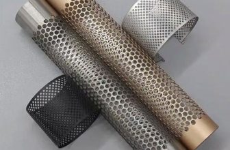
6. Applications of Sub-Micron Features on Stainless Steel
Sub-micron SS features revolutionize: from fuel cells to implants.
Aerospace: Cryo flexures , million cycles.
Biomed: Porous for osseointegration .
Energy: Bipolar plates , >1000 h durability.
Optics: Gratings , sub-µm period.
Precision Micro : radiation meshes, honeycomb arrays.
6.1 Microfluidics and Lab-on-a-Chip
Channels <1 µm for single-cell analysis; SS corrosion-proof .
6.2 Biomedical Devices
Textured implants: Ra 0.1 µm boosts adhesion .
Emitters : CE-MS, 140 µm tips.
6.3 Aerospace and Automotive
Flexures ABS ; injectors .
6.4 Energy and Electronics
Bipolar plates: grooves 50 µm .
Shields, filters .
| Application | Feature Size (µm) | Benefit | Grade | Ref. |
|---|---|---|---|---|
| Microfluidic | 0.5-2 | Flow control | 316L | |
| Implant | 0.2-1 | Biointegration | 304 | |
| Fuel Cell | 50-100 | Conductivity | 316 | |
| Sensor Mesh | 1-10 | Detection | 304 |
Table 6: Applications table.
7. Experimental Procedures and Case Studies
Lab setup: Per , NaCl bath, W tool, oscilloscope monitor.
Case: 304 SS plate, 10V, 100 ns, 1 µm IEG—0.5 µm channels.
Troubleshoot: Bubbles? Increase t_off.
7.1 Step-by-Step Guide
- Prep SS: Polish Ra<0.05 µm.
- Assemble cell.
- Calibrate pulses.
- Etch, rinse.
- Characterize.
7.2 Detailed Case Study: Superhydrophobic Surface
From : 304 SS, NaNO₃, wire cathode, 30V pulses—166° CA.
Conclusion
Challenges: Scale-up, cost of ns generators.
Future: AI pulse optimization, green electrolytes , MXene-SS hybrids.
Sustainability: Recycle electrolytes, per .
PECE on SS: from historical sparks to sub-micron marvels, a testament to ingenuity. As miniaturization marches, this technique promises boundless horizons—durable, precise, transformative.