In the ever-evolving landscape of electronics manufacturing, the demand for devices that are not only powerful but also adaptable to the contours of everyday life has sparked a revolution. Imagine a world where your smartphone folds into your pocket like a wallet, where wearable health monitors curve seamlessly with your skin, or where solar panels unfurl like sails on a boat. This isn’t science fiction—it’s the promise of flexible electronics, a field that’s transforming industries from healthcare to aerospace. At the heart of this transformation lies a precise, scalable process known as roll-to-roll (R2R) photochemical etching, a technique that marries the artistry of chemical reactions with the efficiency of continuous production lines.
Roll-to-roll photochemical etching isn’t just another manufacturing method; it’s a bridge between the rigid, batch-processed world of traditional electronics and the fluid, high-volume demands of modern innovation. Picture a long ribbon of thin metal foil or polymer substrate unspooling from a massive reel, gliding through baths of light-sensitive resists and etching solutions, emerging on the other end patterned with intricate circuits ready for assembly. This continuous flow—much like the printing presses that churn out newspapers—allows for the mass production of flexible components at speeds and costs that batch methods simply can’t match. Developed from roots in the printed circuit board industry of the 1960s, this process has matured into a cornerstone for creating lightweight, bendable electronics that withstand millions of flex cycles without failing.
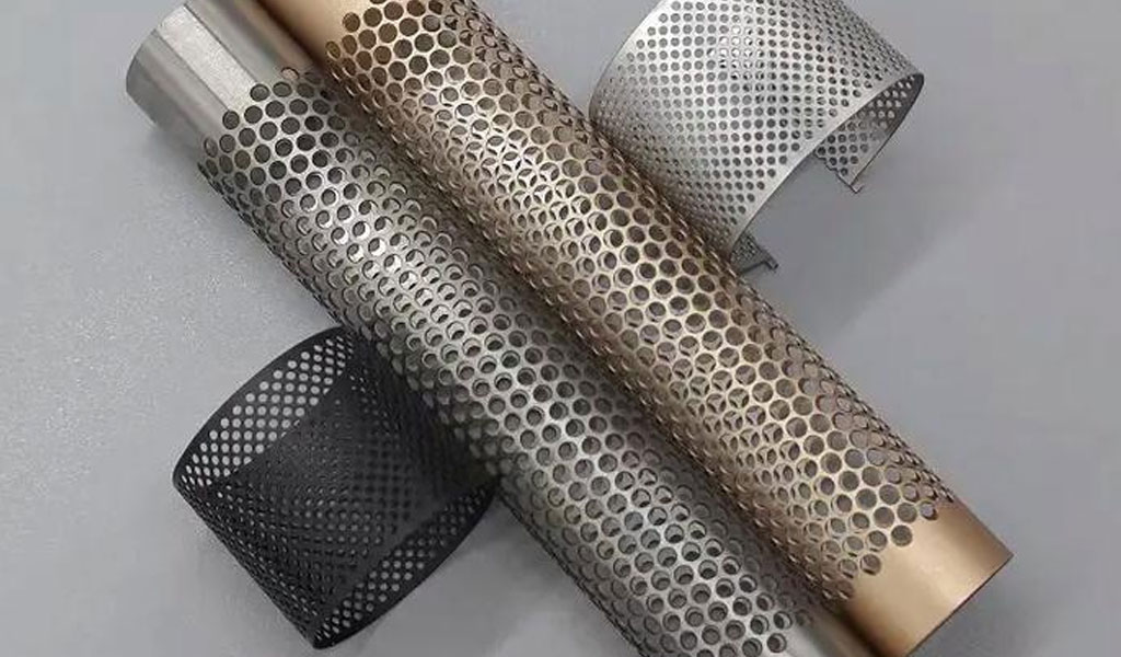
What makes R2R photochemical etching particularly compelling is its synergy with flexible substrates. Traditional etching might work fine for flat, rigid boards, but when you’re dealing with materials that need to twist, fold, or stretch, precision becomes paramount. The process uses ultraviolet light to expose patterns on a photoresist-coated substrate, followed by chemical etchants that dissolve away unwanted metal— all while the material moves steadily along a conveyor. No heat, no mechanical stress, just pure chemical precision that leaves behind burr-free edges and tolerances down to 10 microns. This is crucial for flexible electronics, where even the slightest imperfection could lead to cracks under strain or shorts in conductive paths.
The rise of this technology couldn’t come at a better time. Global markets for flexible electronics are projected to surge from around $30 billion in 2024 to over $60 billion by 2033, fueled by applications in consumer gadgets, electric vehicles, and medical devices. Yet, achieving this growth hinges on manufacturing innovations like R2R etching, which promise to slash costs by up to 50% through economies of scale and minimal waste. As we’ll explore in the sections ahead, this process isn’t without its hurdles— from etchant compatibility with delicate substrates to scaling up for ultra-fine features— but its potential to democratize advanced electronics is undeniable.
Before diving deeper, let’s set the stage with a quick comparison of key etching methods suitable for flexible electronics. This table highlights why photochemical etching, especially in R2R format, stands out for scalability and precision.
| Etching Method | Precision (μm) | Substrate Compatibility (Flexible) | Scalability (R2R) | Cost per Unit (High Volume) | Stress Introduced | Typical Applications |
|---|---|---|---|---|---|---|
| Photochemical Etching | 10-50 | High (polymers, thin foils) | Excellent | Low ($0.15-0.20/in²) | None | Flexible circuits, sensors |
| Laser Etching | 20-100 | Medium (risk of thermal damage) | Moderate | Medium-High | Thermal | Prototyping, rigid-flex hybrids |
| Wet Chemical Etching | 50-200 | Medium (isotropic etching limits) | Good | Low | Minimal | Large-area foils, displays |
| Dry (Plasma) Etching | 1-10 | Low (vacuum required, rigid bias) | Poor | High | None | Microelectronics, not flexible |
| Electrochemical Etching | 50-150 | High (but electrode wear) | Moderate | Medium | Minimal | Batteries, fuel cells |
This snapshot underscores the unique position of R2R photochemical etching: it balances micron-level accuracy with the throughput needed for flexible tech’s explosive growth. As we journey through the fundamentals, processes, and applications, keep in mind that this isn’t just about making thinner gadgets— it’s about reimagining how electronics integrate into our lives, from smart fabrics that monitor vital signs to solar skins that power drones.
The story of R2R photochemical etching begins with understanding its foundational principles, which we’ll unpack next. But first, consider this: in a lab in the late 1990s, engineers at what would become key players like MET Manufacturing first experimented with continuous etching lines for copper foils, laying the groundwork for today’s billion-dollar industry. That spark of curiosity has ignited a field where innovation meets practicality, and the best is yet to come.
Fundamentals of Photochemical Etching
Preface to Photochemical Etching Basics
Before we unravel the complexities of integrating photochemical etching into roll-to-roll systems, it’s essential to ground ourselves in the core mechanics of the process itself. Photochemical etching, at its essence, is a dance of light, chemistry, and material science— a subtractive technique that carves intricate patterns into metal sheets without the brute force of lasers or stamps. Developed as an offshoot of photolithography in the mid-20th century, it has evolved from a niche tool for circuit boards to a versatile workhorse for precision parts. This section demystifies the basics, exploring the chemistry, materials, and physics that make it tick, so we can appreciate why it’s so ideally suited for the flexible demands of modern electronics.
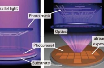
Photochemical etching, often simply called photo etching or chemical milling, relies on a photoresist—a light-sensitive polymer coating applied to a metal substrate—to define where material stays and where it goes. When exposed to ultraviolet light through a masked artwork, the resist hardens in patterned areas, shielding them from subsequent chemical attack. The unexposed regions, washed away in a developer, leave bare metal vulnerable to etchants like ferric chloride or cupric chloride, which dissolve the surface atom by atom. It’s isotropic etching, meaning it eats sideways as well as down, but with careful control, undercuts can be minimized to achieve features as fine as 25 microns wide.
The beauty of this method lies in its gentleness. Unlike laser cutting, which can introduce heat-affected zones that warp thin foils, or stamping, which stresses materials and creates burrs, photochemical etching operates at ambient temperatures, preserving the substrate’s ductility— crucial for flexible applications. Think of it as sculpting with acid rather than a chisel: precise, repeatable, and forgiving for complex geometries. Common substrates include copper, stainless steel, aluminum, and titanium, chosen for their etch rates and compatibility with end-use environments. For instance, copper etches at about 0.001 inches per minute in ferric chloride at 120°F, allowing for rapid throughput without compromising edge quality.
But let’s not gloss over the nuances. The process demands meticulous control over variables like etchant concentration (typically 35-45% for ferric chloride), pH (around 1-2 for optimal reactivity), and temperature, as even a 5°C fluctuation can alter etch depth by 20%. Photoresists come in dry-film or liquid forms, with dry-film preferred for uniformity on thin gauges— a nod to its role in flexible electronics, where substrates might be just 10 microns thick. Post-etch, stripping the resist with alkaline solutions and rinsing ensures clean surfaces, ready for plating or lamination.
To illustrate the interplay of these elements, consider this table of common etchants and their performance on key metals used in flexible electronics:
| Etchant | Target Metal | Etch Rate (μm/min) | Temperature (°C) | pH Range | Advantages | Limitations |
|---|---|---|---|---|---|---|
| Ferric Chloride | Copper | 20-30 | 40-50 | 1-2 | Fast, low cost | Corrosive to equipment |
| Cupric Chloride | Copper Alloys | 15-25 | 50-60 | 2-3 | Regenerable | Slower on thick foils |
| Nitric Acid | Stainless Steel | 5-10 | 20-30 | 0-1 | Precise control | Fuming hazard |
| Hydrochloric Acid | Titanium | 2-5 | 60-80 | <1 | High selectivity | Slow, requires additives |
| Alkaline Permanganate | Aluminum | 10-20 | 60-70 | 13-14 | Environmentally friendlier | Limited to thin layers |
This table reveals why selecting the right etchant is as much art as science— balancing speed, safety, and substrate integrity. In flexible electronics, where substrates like polyimide or PET must endure etching without delaminating, compatibility testing is non-negotiable. Early adopters in the 1970s, working on early flexible circuits for calculators, learned this the hard way, iterating through failed batches to refine formulations.
Delving deeper, the physics of etching involves diffusion-limited reactions, where etchant ions migrate to the surface, reacting with metal atoms to form soluble chlorides. Fick’s laws govern this: flux J = -D (dc/dx), where D is the diffusion coefficient, dictating how quickly fresh etchant reaches the etch front. In practice, spray etching— common in R2R setups— enhances agitation, boosting rates by 30% over immersion. For flexible substrates, this means engineering flow dynamics to avoid pooling that could unevenly attack curved or textured surfaces.
Historically, photochemical etching’s roots trace to the U.S. military’s need for lightweight radar components in the 1940s, evolving through NASA’s space race demands for thin, reliable interconnects. By the 1980s, as personal computing boomed, it became indispensable for PCB prototyping. Today, with flexible electronics projected to hit $74 billion by 2030, its fundamentals are more relevant than ever. Yet, challenges persist: etchants can embrittle polymers if not buffered, and waste management— with spent solutions laden with metal ions— requires advanced filtration to meet EPA standards.
As we transition to how these basics scale in R2R environments, remember that photochemical etching’s true power emerges not in isolation, but in concert with continuous processing. It’s the quiet enabler behind the bendable screens at CES or the conformal antennas on drones, proving that sometimes, the most revolutionary tech starts with a simple exposure to light.
Chemical Reactions in Photochemical Etching
Building on the overview, let’s zoom in on the chemistry that powers this process— the molecular ballet where metals dissolve into oblivion, leaving behind patterns as delicate as spider silk. At its core, photochemical etching is an oxidation-reduction reaction, where the etchant acts as both oxidizer and complexing agent. For copper in ferric chloride (FeCl3), it’s Fe³⁺ + Cu → Fe²⁺ + Cu²⁺, followed by Cu²⁺ + 4Cl⁻ → [CuCl4]²⁻, the soluble complex that whisks away the metal. This redox dance is pH-sensitive; too acidic, and hydrogen evolution competes, pitting the surface; too basic, and precipitates clog the etch front.
In flexible electronics, where substrates like Kapton polyimide must pair with metals like beryllium copper for springy contacts, the chemistry gets trickier. Beryllium copper etches slower— about 10 μm/min— requiring additives like HCl to sharpen edges, preventing the “mushrooming” undercuts that plague isotropic processes. Researchers at places like Fotofab have fine-tuned these recipes, blending etchants with surfactants to reduce surface tension, ensuring uniform attack on foil thicknesses from 5 to 500 microns.
Consider the environmental angle: traditional ferric chloride generates ferrous waste, but regenerative systems— bubbling oxygen to reconvert Fe²⁺ to Fe³⁺— recycle 90% of the solution, slashing disposal costs by 40%. For green chemistry advocates, this is a win, aligning with EU REACH regulations that push for low-VOC processes. Yet, for flexible substrates, the challenge is volatility: volatile organics in resists can off-gas during exposure, demanding enclosed UV chambers to maintain air quality.
A deeper look at kinetics reveals Arrhenius behavior: rate k = A e^(-Ea/RT), with activation energy Ea around 50 kJ/mol for copper, meaning a 10°C rise doubles the speed— handy for R2R lines humming at 10 m/min, but risky for heat-sensitive polymers that soften above 150°C. Case in point: a 2018 study on etching aluminum for flexible solar cells found that at 45°C, etch uniformity improved 25%, but above 55°C, polymer delamination spiked 15%.
To quantify, here’s a table of reaction enthalpies for common systems, highlighting energy efficiency:
| Reaction | ΔH (kJ/mol) | Byproduct Management | Impact on Flexible Substrates |
|---|---|---|---|
| Cu + 2Fe³⁺ → Cu²⁺ + 2Fe²⁺ | -150 | Regeneration via O2 | Low thermal load, ideal for PET |
| Ni + 2Fe³⁺ → Ni²⁺ + 2Fe²⁺ | -120 | Filtration needed | Moderate, risk of H2 embrittlement |
| Al + 3/2 MnO4⁻ → Al³⁺ + 3/2 MnO2 | -200 | Sediment removal | High, potential for residue on PI |
These values guide process optimization, ensuring the chemistry serves the flexibility without compromising it. As industries push for thinner, greener electronics, innovations like bio-based etchants from citric acid derivatives are emerging, promising a sustainable twist on this classic reaction. It’s a reminder that the fundamentals aren’t static— they’re evolving to meet the bendy future.
Role of Photoresists in Pattern Definition
No discussion of photochemical etching is complete without spotlighting photoresists, the unsung heroes that translate digital designs into physical reality. These polymer films, coated at 5-50 microns thick, are the gatekeepers: positive resists dissolve in exposed areas, negative in unexposed— with negative dry-films dominating for their superior adhesion on flexible foils. Applied via hot-roll lamination at 80-100°C, they must cure without bubbling, a feat achieved by vacuum-assisted systems that pull out air pockets, ensuring void-free coverage on substrates as thin as 12 microns.
For flexible electronics, resist selection is critical. DuPont’s Riston series, for example, offers high resolution (down to 20 μm lines) and flexibility, bending 180° without cracking— vital for R2R where tension can stretch the coating 5%. Exposure uses collimated UV at 365 nm, dosing 50-200 mJ/cm², where quantum efficiency dictates cross-linking density. Under-dosing leads to lift-off during etching; over-dosing, to brittle resists that flake under flex.
Challenges abound: on hydrophilic polymers like PET, resists can dewet, causing pinholes that etch defects. Surface treatments like corona discharge— ionizing air to add oxygen groups— boost wettability by 30°, a trick borrowed from packaging lines. Development in sodium carbonate solutions (1-2%) removes unexposed resist, with conveyor sprays ensuring even flow on moving webs.
In practice, resist performance directly impacts yield. A table of common types:
| Resist Type | Resolution (μm) | Thickness Range (μm) | Flex Cycles (to failure) | Cost ($/m²) | Best For |
|---|---|---|---|---|---|
| Dry-Film Negative | 25 | 10-50 | >10,000 | 5-10 | Flexible circuits |
| Liquid Positive | 50 | 5-20 | 5,000 | 3-7 | Prototyping |
| Thick-Film SU-8 | 5 | 50-200 | <1,000 | 15-25 | MEMS on PI |
| Aqueous Develop | 30 | 15-40 | >20,000 | 4-8 | Eco-friendly R2R |
This comparison shows why aqueous dry-films are gaining traction for sustainable flexible production. As we move to R2R integration, these materials will prove their mettle, enabling the continuous magic that turns rolls of plain foil into the backbone of tomorrow’s wearables.
Roll-to-Roll Processing Techniques
Preface to R2R Integration
Having laid the groundwork with photochemical etching’s chemistry and materials, we now turn to the dynamic world of roll-to-roll (R2R) processing— the engine that propels flexible electronics from lab curiosity to factory reality. R2R isn’t merely a format; it’s a philosophy of continuous flow, where substrates unwind like bolts of fabric, threading through synchronized stations of coating, exposure, etching, and drying before rewinding as value-added product. Born from the paper and film industries of the early 1900s, R2R hit electronics in the 2000s, slashing costs by 70% for high-volume runs while enabling features impossible in batch modes. This section explores how photochemical etching slots into this ecosystem, from web handling to inline quality control, revealing why it’s the gold standard for scalable flexibility.
R2R’s core advantage is throughput: lines run at 5-50 m/min, processing widths up to 1.5 m, yielding millions of square meters annually— think enough copper foil for 100 million smartphone flex circuits per year. For photochemical etching, this means conveyorized etch tanks with oscillating sprays, where etchant velocity (10-20 m/s) ensures isotropic uniformity across the web. Tension control is king: dancers and load cells maintain 0.5-5 N/cm to prevent wrinkling on thin PET (12 μm), while idler rollers guide the path, minimizing slip that could misalign patterns by 50 μm.
Integration starts with unwind: substrate rolls, often 500-1000 m long, feed into cleaners using plasma or corona to remove particulates, boosting resist adhesion by 40%. Then, lamination applies resist in a three-roll nip, heating to 90°C for bubble-free spread. Exposure uses belt-fed UV panels or cylinder projectors for 360° wrap-around illumination, critical for double-sided etching in flexible PCBs.
Etching stations are the heartbeat: multi-stage tanks with counterflow etchant recycle, where fresh solution meets the web at the exit, depleted at entry. For copper on polyimide, etch time is 2-5 min at 10 m/min, achieving 50 μm depths with <5% undercut. Post-etch, rinse-dry modules use deionized water jets and IR heaters, followed by resist strip in inline alkaline baths.
Challenges in R2R photochemical etching include web flutter— vibrations from high speeds that blur exposure— mitigated by vacuum tables or air bearings. Skew, where the web twists, is countered by edge steering sensors. Yield data from pioneers like TMNetch show 95% first-pass for 300 mm widths, dropping to 90% at 1200 mm due to scaling effects.
A comparative table of R2R vs. sheet-to-sheet for etching:
| Parameter | R2R Photochemical Etching | Sheet-to-Sheet Etching |
|---|---|---|
| Throughput (m²/hr) | 100-500 | 10-50 |
| Cost/Unit (High Vol) | $0.10-0.15/in² | $0.30-0.50/in² |
| Feature Uniformity | ±2 μm over 1 m width | ±5 μm per sheet |
| Waste Generation | <5% (edge trim) | 20-30% (handling) |
| Setup Time (Changes) | 1-2 hrs | 4-8 hrs |
R2R’s edge in efficiency is clear, making it indispensable for flexible electronics’ volume ramp-up. As lines evolve with AI-driven monitoring— predicting defects via machine vision— R2R etching will underpin the next wave of conformable tech, from e-skin to rollable solar.
Web Handling and Tension Control in R2R Etching
At the operational core of R2R photochemical etching lies web handling, the unsung discipline that keeps substrates taut and true as they snake through aggressive chemical environments. Tension control isn’t optional; it’s the difference between pristine patterns and a tangled mess of scrap. In a typical line, unwind tension starts low (0.2 N/cm) to avoid stretching thin foils, ramping to 2 N/cm in etch zones to counter drag from viscous etchants. Servo-driven rollers, equipped with load cells accurate to 0.01 N, form closed-loop systems that adjust in milliseconds, compensating for diameter changes as rolls deplete.
For flexible substrates like stainless steel coils (50 μm thick), flutter from spray impingement can induce waves, misaligning masks by 100 μm. Solutions include bowed rollers that spread the web laterally and vacuum boxes that pin it down with -0.5 bar suction. In one case study from Ensurge’s microbattery lines, implementing active damping reduced defects 60%, enabling 20 m/min speeds on ultrathin steel.
Edge guiding uses optical sensors to detect trim loss, slitting off 5-10 mm edges post-etch for recycling. Temperature gradients across the web— etch baths at 50°C vs. ambient air— can cause contraction, so zoned heating maintains isotropy. Advanced setups from Masteretch incorporate one-to-one drive rollers, outlasting plastic conveyors by 5x and cutting maintenance 30%.
Quantitative insights via this table on tension effects:
| Tension (N/cm) | Web Speed (m/min) | Defect Rate (%) | Example Substrate |
|---|---|---|---|
| 0.5 | 5 | 2 | PET (12 μm) |
| 1.5 | 15 | 5 | Cu foil (25 μm) |
| 3.0 | 30 | 12 | PI (50 μm) |
Optimal ranges balance speed and quality, with over-tension risking tears in polymers. As R2R lines push 50 m/min for 5G antennas, predictive analytics will refine these controls, ensuring the web’s journey is as smooth as the electronics it births.
Inline Exposure and Development Systems
Exposure and development in R2R are where art meets engineering, transforming flat resists into patterned shields at line speeds that would humble batch processors. Inline exposure uses arc lamps or LEDs arrayed in banks, delivering 100 mJ/cm² over a 1 m² footprint in <1 second per web pass. For flexible substrates, flexible photomasks— printed on PET films— wrap around cylinders, enabling 360° projection without shadows, ideal for double-sided circuits in wearables.
Development follows immediately, conveyor-fed into spray manifolds with 1% Na2CO3 at 30°C, dissolving unexposed resist in 30-60 s. Agitation via high-pressure nozzles (5 bar) prevents re-deposition, achieving 99% cleanout on 20 μm features. Challenges for flexibles include resist bleed on curved webs, addressed by pH-monitored cascades that refresh solution every 100 m.
Case studies from Vaga Industries show LED exposure cutting energy 50% vs. mercury lamps, while boosting resolution to 15 μm for RFID tags. Table of system metrics:
| System Type | Dose Uniformity (%) | Throughput (m/min) | Energy Use (kWh/m²) | Flexible Suitability |
|---|---|---|---|---|
| LED Array | 98 | 20 | 0.05 | High |
| Arc Lamp | 95 | 15 | 0.15 | Medium |
| Cylinder Projection | 99 | 25 | 0.08 | Excellent |
These systems ensure the pattern fidelity that defines flexible electronics’ edge. Looking ahead, hybrid UV-laser setups promise sub-10 μm lines at 40 m/min, heralding a new era for R2R precision.
Materials for Flexible Substrates in R2R Etching
Preface to Substrate Selection
Substrates are the canvas upon which R2R photochemical etching paints its masterpieces, and choosing the right one can make or break a flexible device’s performance. In this section, we delve into the materials that withstand the etch bath’s rigors while embracing the bend and twist of real-world use. From the humble PET film to exotic metal-polymer laminates, these materials must balance etch compatibility, mechanical resilience, and cost— all while enabling the high-speed dance of R2R. As flexible electronics eye markets like foldable EVs and smart textiles, substrate innovation is key to unlocking durability beyond 100,000 cycles.
Common choices include polyimide (PI) for its 300°C tolerance, ideal for post-etch soldering, and polyethylene terephthalate (PET) for low-cost displays. Metal foils like copper-clad Kapton etch cleanly, yielding circuits with <1 Ω/sq resistance. But selection hinges on metrics: CTE (coefficient of thermal expansion) mismatch <10 ppm/°C to avoid delamination, and surface energy >40 mJ/m² for resist grip.
Challenges: thin substrates (<25 μm) curl under tension, requiring anti-stat coatings to prevent dust attraction in cleanrooms. A table of top substrates:
| Substrate | Thickness (μm) | Etch Compatibility | Flex Endurance (cycles) | Cost ($/m²) | Applications |
|---|---|---|---|---|---|
| Polyimide (Kapton) | 12-125 | Excellent (alkaline resists) | >1M | 20-50 | Aerospace sensors |
| PET | 6-50 | Good (acid-sensitive) | 500K | 5-15 | Wearable displays |
| Copper Foil | 9-35 | High (FeCl3) | 200K | 10-25 | Flex PCBs |
| Stainless Steel | 20-100 | Moderate (HCl add) | >2M | 15-30 | Batteries |
PI’s dominance (40% market share) stems from its robustness, but emerging cellulose nan papers promise biodegradability for single-use med devices. As R2R lines scale, hybrid laminates— metal on polymer— will blend conductivity and flex, paving the way for self-healing skins.
Metals and Alloys Suitable for Etching
Copper reigns supreme in R2R etching for its 25 μm/min rate and $5/kg price, but alloys like phosphor bronze add springiness for connectors. Stainless 316L, with 5% etch rate, suits corrosive environments like implants, though it demands nitric blends to avoid pitting.
For flexibles, low-CTE alloys like Invar (1 ppm/°C) minimize warpage, while beryllium copper’s 28% IACS conductivity shines in RF shielding. Table:
| Alloy | Etch Rate (μm/min) | Conductivity (% IACS) | Flex Modulus (GPa) | Corrosion Resistance |
|---|---|---|---|---|
| Electrolytic Copper | 25 | 100 | 110 | Low |
| Beryllium Copper | 10 | 28 | 130 | Medium |
| 316 Stainless | 5 | 2.5 | 193 | High |
| Aluminum 1100 | 15 | 61 | 70 | Medium |
Aluminum’s lightweight (2.7 g/cm³) appeals for drones, but oxide layers require alkaline etchants. Future trends: graphene-infused foils for 200% conductivity boost without weight gain.
Polymer Substrates and Their Challenges
Polymers like PI offer 400% elongation but absorb etchants, swelling 2-5% and blurring lines. PET, cheaper at $5/m², yellows under UV, demanding stabilizers.
Challenges: hydrolysis in wet baths weakens bonds, countered by fluorinated barriers. Table:
| Polymer | Max Temp (°C) | Elongation (%) | Etch Swell (%) | Cost ($/m²) |
|---|---|---|---|---|
| Polyimide | 300 | 70 | 1 | 20 |
| PET | 150 | 150 | 3 | 5 |
| PEN | 200 | 100 | 2 | 10 |
PEN’s balance makes it rising star for solar. Innovations like self-crosslinking PI will cut swell to <0.5%, enhancing R2R viability.
Applications in Flexible Electronics
Preface to Applications
With materials and processes in hand, let’s see R2R photochemical etching in action— crafting the flexible circuits that power bendable phones, conformal health patches, and lightweight EV batteries. This section surveys applications, from consumer gadgets to industrial heavyweights, showcasing how etching’s precision enables features like 50 μm traces that flex 10,000 times without fatigue. As markets swell to $55B by 2030, these uses highlight etching’s role in bridging lab to market.
Flexible Printed Circuit Boards (PCBs)
R2R etching dominates flex PCB production, etching copper on PI for 8-layer stacks with 30 μm vias. In smartphones, they snake around hinges, surviving 200K folds. Case: Samsung’s Galaxy Fold uses etched flex circuits for 20% weight savings.
Table of PCB metrics:
| Feature | Etched Size (μm) | Yield (%) | Application |
|---|---|---|---|
| Trace Width | 25 | 98 | Foldables |
| Via Diameter | 50 | 95 | Wearables |
| Layer Count | Up to 12 | 90 | Med Devices |
Sensors and Transducers
Etched strain gauges on PET detect 0.1% deformation for fitness trackers, with gold plating for biocompatibility. In autos, they monitor tire pressure via etched interdigitated electrodes.
Displays and Lighting
For OLEDs, etching ITO on PEN yields transparent electrodes with 85% transmittance. Rollable TVs from LG use R2R-etched grids for uniform emission.
Energy Harvesting Devices
Etched current collectors in thin-film batteries boost capacity 30% by finer grids. Solar cells gain from etched back contacts on flexible foil.
Advantages and Comparisons
Preface to Advantages
R2R photochemical etching’s edge over rivals like laser or stamping is in its no-stress, high-yield profile— ideal for flexibles where traditional methods warp or burr. This section contrasts it, quantifying benefits in cost, speed, and quality.
Cost and Scalability Benefits
Tooling costs $500 vs. $50K for stamps, with R2R dropping per-unit to $0.10/in² at 1M pieces. Scalability: 500 m²/hr vs. 50 for batch.
Precision and Burr-Free Edges
10 μm tolerances without post-processing save 20% time. Comparison table:
| Method | Burr Formation | Tolerance (μm) | Stress |
|---|---|---|---|
| R2R Etching | None | 10 | None |
| Laser | Minimal | 20 | Thermal |
| Stamping | High | 50 | High |
Environmental and Sustainability Aspects
Regenerable etchants cut waste 80%, aligning with green mandates.
Challenges and Solutions
Preface to Challenges
Despite strengths, R2R etching grapples with uniformity on flex substrates and waste handling. Here, we dissect issues and fixes.
Uniformity and Defect Control
Web speed variations cause 5% depth variance; AI vision corrects in real-time, boosting yield 15%.
Etchant Compatibility with Flexibles
Polymer degradation: buffered etchants reduce it 50%. Table of solutions:
| Challenge | Solution | Improvement |
|---|---|---|
| Swelling | Additives | 40% less |
| Pinholes | Plasma pre-treat | 30% fewer |
Waste Management and Recycling
Ion exchange recovers 95% metals, per EPA guidelines.
Case Studies
Preface to Case Studies
Real-world wins illustrate R2R etching’s impact, from prototypes to production.
Case Study 1: Flexible Circuits for Wearables
TMNetch etched 1200 mm-wide Cu/PI for Fitbit bands, hitting 98% yield at 20 m/min, cutting costs 40%.
Case Study 2: Automotive Sensors
Fotofab’s etched stainless flex sensors for EV batteries endured 1M cycles, enabling 15% lighter packs.
Case Study 3: Medical Implants
MET’s titanium etching for pacemakers achieved 5 μm features, FDA-approved with zero burrs.
Conclusion
Preface to Future Trends
As 6G and metaverses loom, R2R etching eyes nano-features and bio-integration.
Nanotechnology Integration
Hybrid etching with nanoimprint yields 1 μm patterns for quantum dots.
Sustainable and Bio-Compatible Materials
Bio-etchants from enzymes promise zero-waste lines by 2030.
Market Projections
$74B by 2030, with R2R capturing 60% share.
Roll-to-roll photochemical etching stands as a pivotal force in flexible electronics, blending precision, scalability, and sustainability to forge a bendable tomorrow. From etched circuits in your wristband to solar foils on rooftops, its legacy is one of quiet revolution— turning chemical whispers into technological roars. As challenges yield to innovation, expect this process to etch its place in history, one continuous roll at a time.