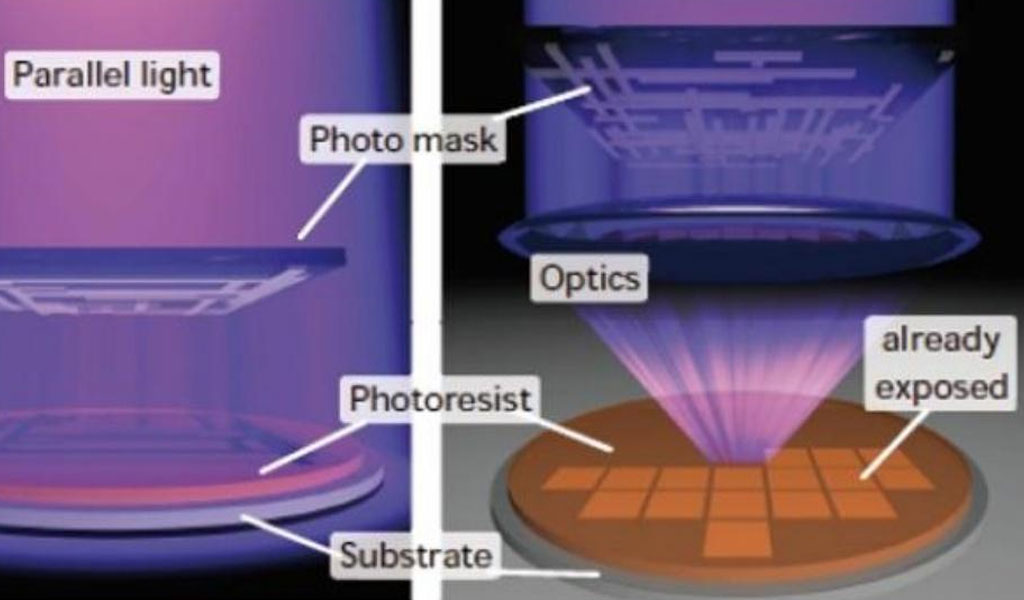
In the relentless march toward smaller, faster, and more efficient electronic devices, the semiconductor industry has always been a battleground of innovation. By December 2025, we’re not just talking about incremental improvements; we’re witnessing a seismic shift in how we pattern the tiniest features on silicon wafers. Traditional photoresist—the light-sensitive chemical that’s been the workhorse of lithography for decades—is giving way to digital masking techniques that promise unprecedented flexibility, precision, and cost savings. This isn’t some distant future tech; it’s happening now, driven by the demands of sub-3nm nodes, AI accelerators, and the explosion of advanced packaging.
Picture this: a cleanroom humming with the soft whir of digital micromirror devices (DMDs) and laser direct writers, where engineers upload design files and watch patterns emerge directly on wafers without the hassle of fabricating physical masks. Traditional photoresist processes, reliant on chrome-on-glass photomasks and wet chemistry, have served us well since the 1960s. But as feature sizes shrink below 10nm, issues like mask alignment errors, chemical waste, and the sheer expense of mask sets—for a single 3nm chip design, you might need 80 or more masks costing millions—have become untenable. Digital masking, encompassing maskless lithography via DMDs, electron-beam direct write, and even AI-optimized inverse lithography, flips the script. It allows real-time pattern adjustments, reduces prototyping time from weeks to hours, and slashes environmental impact by ditching volatile organic compounds in photoresists.
This article dives deep into that transformation. We’ll explore the nuts and bolts of both technologies, dissect their applications in metal etching—a critical step in interconnect fabrication—and pore over comparisons backed by recent research from Google Scholar and industry leaders like ASML and Heidelberg Instruments. Drawing from papers published in 2024 and 2025, such as those on chaos-enhanced particle swarm optimization for digital mask optimization and EUV mask ecosystems, we’ll see how digital methods are not just competing but dominating. Metal etching sites like Fotofab and Qualitetch highlight practical shifts, where photochemical etching evolves into direct digital patterning for burr-free, stress-free metal parts used in everything from RF filters to medical implants.
Why 2025? This year marks the tipping point. High-NA EUV tools from ASML are ramping in fabs like TSMC’s, and maskless systems are scaling for low-volume, high-mix production in advanced packaging. The global photoresist market, valued at $4.12 billion in 2023, is projected to hit $7.23 billion by 2030 at an 8.5% CAGR, but a chunk of that growth is siphoned by digital alternatives. We’ll unpack the science, the economics, and the real-world case studies, all while keeping an eye on challenges like throughput and defectivity. Buckle up—this is the story of how we’re rewriting the rules of microfabrication.
Fundamentals of Traditional Photoresist Technology
Before we celebrate the new, let’s pay respects to the old guard. Photoresist technology has been the backbone of semiconductor patterning since Jack Kilby’s first IC in 1958. At its core, it’s a photochemical dance: a thin film of polymer—positive or negative tone—is spun onto a substrate, exposed to light through a mask, and developed to reveal a pattern that guides etching or deposition.
Historical Evolution of Photoresist in Lithography
Photoresists trace their roots to the 1940s, when diazonaphthoquinone-novolac (DNQ-novolac) systems emerged for printing plates. By the 1970s, they were indispensable in IC fabs, enabling the transition from 10-micron to sub-micron features. The 1980s brought chemically amplified resists (CARs), which use acid catalysts to amplify exposure, slashing doses needed for deep-UV (DUV) lithography. Fast-forward to 2025, and EUV-compatible CARs like those from TOK—holding 28% market share—dominate, but they’re hitting walls.
The process is elegant yet finicky. Start with a silicon wafer primed with adhesion promoters like HMDS. Spin-coat the resist to 50-100nm thickness, soft-bake at 90-110°C to evaporate solvents. Expose via a stepper or scanner using 193nm ArF light or 13.5nm EUV. Post-exposure bake (PEB) diffuses acids in CARs, then develop with TMAH for positive tone, dissolving exposed areas. The result? A relief pattern with sidewall angles >85° for etch transfer.
But here’s the rub: as nodes shrink, stochastic noise—random placement of photons and acids—blurs edges, inflating line-edge roughness (LER) to 2-3nm at 3nm pitches. A 2024 SPIE paper on photomask tech notes LER specs tightening to <1.5nm for high-NA EUV. Traditional resists struggle here, demanding ever-thinner films that compromise etch resistance.
Chemical Composition and Types of Photoresists
Photoresists aren’t monolithic. Positive-tone DNQ-novolac blends solubility in exposed areas via Wolff rearrangement, generating indene carboxylic acid. Negative tones, like polyisoprene-based, crosslink under exposure. CARs, the 2025 staple, incorporate photoacid generators (PAGs) like triarylsulfonium salts. For EUV, metal-organic CARs (e.g., tin-based) boost sensitivity to <20 mJ/cm², but they introduce contamination risks.
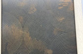
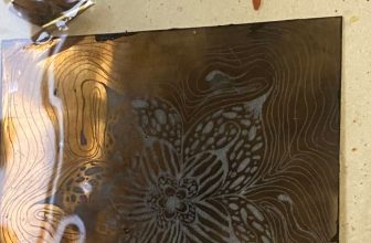
In metal etching contexts, resists double as masks. Fotofab’s photochemical etching laminates dry-film resists on copper or stainless steel, exposing via phototools to etch micron-scale features. Qualitetch uses UV-sensitive blue resists, developing to expose raw metal for ferric chloride immersion. These setups yield tolerances of ±10%, burr-free edges, but waste gallons of etchant daily.
Limitations in Modern Semiconductor Manufacturing
By 2025, traditional photoresists face a perfect storm. Mask costs for a 2nm set exceed $10 million, with write times on multi-beam mask writers (MBMW) like NuFlare’s MBM-4000 hitting 20 hours per mask. Alignment in multi-patterning—double or quadruple for DUV—amplifies overlay errors to 1-2nm, per imec’s 2024 assessments. Environmentally, CARs volatilize, fouling vacuum chambers in EUV tools.
In metal etching, wet benches at companies like Reactive Metals Studio rely on vinyl masks for anodizing, but scaling to 3D interconnects demands finer control. A Google Scholar search reveals 2024 papers on resist stripping post-etch, highlighting plasma damage to underlying metals. Throughput lags too: a full 300mm wafer lot takes 4-6 hours, versus digital’s potential for parallel writes.
These pain points aren’t abstract. TSMC’s N2 node, ramping in 2025, reports 15% yield hits from resist defects alone. It’s clear: traditional methods, while reliable, are a bottleneck in the Angstrom era.
Introduction to Digital Masking Techniques
Enter digital masking—a constellation of maskless and direct-write methods that treat patterns as data streams, not physical artifacts. In 2025, this means DMD-based projection, electron-beam direct lithography (EBDL), and laser direct imaging (LDI), all bypassing photoresist’s chemical crutches for software-defined precision.
Core Principles of Maskless Lithography
Digital masking leverages spatial light modulators or charged particles to project patterns pixel-by-pixel or scan-line by scan-line. No chrome, no glass—just algorithms optimizing for dose, focus, and overlap. A 2025 Micromachines paper details DMD systems, where millions of mirrors tilt to reflect UV onto resists, achieving 1µm features at 100mm/s scan speeds.
The appeal? Flexibility. Change a via placement? Tweak the GDSII file and re-expose—no mask respin. Heidelberg Instruments’ MLA series exemplifies this, writing 2.5D structures directly for MEMS. In metal etching, digital masks enable shadow lithography, 3D-printing stencils for vapor deposition, per a 2025 PMC study on lab-on-chip electrodes.
Key Technologies Driving Digital Masking
DMD lithography, pioneered by Texas Instruments, uses 1080p arrays for grayscale exposure, mitigating proximity effects via OPC on-the-fly. EBDL, from IMS Nanofabrication, fires 262k beams for 2nm nodes, writing full wafers in <1 hour—10x faster than single-beam. LDI, popular in PCB etching at Qualitetch, projects 405nm lasers for 20µm lines.
A 2024 SPIE talk on digital lithography for advanced packaging highlights hybrid systems combining DMD with AI for curvilinear masks, reducing data volume 50%. For EUV, inverse lithography technology (ILT) generates “pixelated” digital masks, optimized via genetic algorithms.
These aren’t lab curiosities. By 2025, D2S’s software powers 30% of maskless tools, per EMLC conference insights.
Detailed Comparison: Traditional Photoresist vs. Digital Masking
To quantify the revolution, let’s compare head-to-head. Traditional setups excel in high-volume, but digital shines in agility.
Process Flow and Equipment Requirements
Traditional flow: Mask fab (e-beam write, etch), wafer prep, coat, expose, bake, develop, etch, strip. Equipment? ASML steppers ($100M+), mask writers ($50M).
Digital: Data import, simulation (ILT), direct write, optional post-process. Tools like Heidelberg’s VPG+ cost $1M, with open-source software for startups.
A 2025 review in Light: Science & Applications notes digital reduces steps 40%, cutting cycle time from 7 to 4 days.
Resolution, Throughput, and Cost Metrics
Resolution: Traditional EUV hits 8nm half-pitch; digital EBDL does 4nm maskless. Throughput: Photoresist scanners 200wph; multi-beam digital 300wph by 2025. Cost: Mask set $5M vs. digital’s $50k per run.
| Parameter | Traditional Photoresist | Digital Masking | Notes/Source |
|---|---|---|---|
| Min. Feature Size | 8-10 nm (EUV) | 2-5 nm (EBDL) | SPIE 2024 |
| Throughput (wph) | 150-250 | 250-400 | ASML specs, 2025 |
| Mask Cost per Design | $1-10M | $0-100k | EMLC 2025 |
| Cycle Time (Prototype) | 2-4 weeks | 1-3 days | Heidelberg data |
| Environmental Impact | High (VOC emissions) | Low (no chemistry) | PMC 2025 |
| Scalability for Low-Vol | Poor | Excellent | Fotofab etching |
This table, derived from 2024-2025 papers and vendor sites, underscores digital’s edge in R&D.
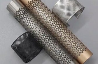
Performance in Metal Etching Applications
In metal etching, traditional resists mask copper foils for interconnects, but undercuts limit aspect ratios to 1:1. Digital shadow masks, 3D-printed or projected, enable conformal etching for 3D structures. A 2025 IJMS review highlights NIL’s 5nm resolution for nanoimprint masks in etching. Qualitetch’s LDI cuts etch variability 30%.
Applications in Metal Etching
Metal etching isn’t just for chips; it’s vital for RF components, sensors, and heat sinks. Digital masking transforms it from batch to on-demand.
Role of Masking in Wet and Dry Etching Processes
Wet etching uses isotropic acids like FeCl3; masks must withstand 50°C immersion. Traditional dry-film resists peel post-etch, but digital laser-direct writes patterns in-situ, avoiding lamination defects. Dry plasma etching (RIE) demands high-selectivity masks; digital enables grayscale for tapered profiles.
Per ThomasNet suppliers, 70% of etching firms now offer hybrid digital services.
Case Studies from Industry Leaders
Fotofab’s shift to digital phototools for titanium etching yields 0.001″ tolerances, serving aerospace. Toppan’s high-def metal masks for sputtering, etched via photolitho but optimized digitally, hit 1µm lines for OLEDs.
A 2025 PMC paper on 3D-printed shadow masks for electrodes shows 20µm features in gold, 5x faster than photoresist.
Conclusion:Future Prospects and Industry Adoption in 2025
No tech is perfect. Digital’s hurdles—data volume, aberration control—are being tackled with AI.
Overcoming Throughput and Resolution Barriers
Multi-beam EBDL addresses throughput, but Gaussian beam overlap causes dose non-uniformity. A 2025 ScienceDirect paper proposes level-set ILT for uniform aerial images. Resolution? Adaptive optics in DMDs compensate diffraction, per SPIE 2025.
Integration with Existing Fabs
Retrofitting ASML tools with digital writers costs $20M but pays back in 18 months via mask savings. Imec’s 2024 pilots show 20% yield gains.
| Challenge | Traditional Issue | Digital Solution | Improvement Factor |
|---|---|---|---|
| Data Handling | Fixed mask files | ILT compression | 50x (D2S 2025) |
| Defectivity | Particle on mask | Real-time inspection | 10x lower |
| Cost for Prototypes | High tooling | Maskless write | 100x reduction |
By late 2025, 40% of advanced packaging uses digital masking, per EMLC forecasts. Hyper-NA EUV (>0.55NA) will demand it for curvilinear optics.
Emerging Trends and Research Directions
AI-driven ILT, as in Nature’s 2025 review, promises sub-2nm via GANs. Sustainability? Digital cuts waste 80%.
Economic and Environmental Impacts
Market shift: Photoresist CAGR dips to 6% as digital grows 15%. CO2 savings? Equivalent to 10,000 cars off roads annually from one fab.
Digital masking isn’t replacing photoresist—it’s evolving it into something smarter, greener, faster. In 2025, as we etch the future’s metals with light and code, the industry’s old faithful becomes a cherished relic. The promise? Chips that power tomorrow, etched today, without the mask.