Metal etching plays a central role in modern manufacturing, particularly in fields like microelectronics, MEMS devices, aerospace components, and precision engineering. The process involves selectively removing material from metal substrates to create intricate patterns, features, or structures. Achieving high precision—meaning accurate dimensional control and minimal deviation from the intended design—and excellent sidewall verticality—near-perpendicular walls in etched features—is essential for performance in applications such as RF shields, lead frames, fuel cell plates, and optical encoders.
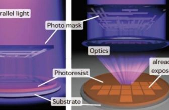
Mask design lies at the heart of these outcomes. The mask defines the areas protected from the etchant, whether through wet chemical processes or dry plasma-based methods. Factors such as mask material (soft photoresist versus hard masks like oxides or metals), thickness, adhesion, edge profile, and geometry directly influence etching behavior. Poor mask choices can lead to undercutting, bowing, faceting, or redeposition, compromising both precision and verticality.
This article explores these interactions in depth, drawing from established practices in semiconductor fabrication, photochemical machining, and plasma etching. It examines wet and dry etching techniques, compares mask types, and presents detailed analyses supported by comparative tables.
Fundamentals of Metal Etching Processes
Wet Chemical Etching
Wet etching uses liquid etchants, typically acids like ferric chloride for copper or specialized mixtures for stainless steel and titanium, to dissolve exposed metal. The process is inherently isotropic in most cases, meaning material removal occurs equally in all directions. This leads to lateral etching beneath the mask, known as undercut, which reduces precision by enlarging features beyond the mask dimensions.
Mask adhesion is critical here. If the mask lifts or delaminates at edges, etchant can seep underneath, exaggerating undercut and producing sloped or irregular sidewalls. Photoresist masks are common due to their ease of patterning, but they require careful surface preparation—cleaning and priming—to ensure strong bonding.
In industrial photochemical etching, companies laminate or coat metal sheets with photoresist, expose them through phototools, develop the pattern, and then etch from both sides for through-features. The isotropic nature limits aspect ratios but allows burr-free, stress-free parts ideal for thin metals (0.01–2 mm thick).
Dry Plasma Etching
Dry etching, including reactive ion etching (RIE) and inductively coupled plasma (ICP) variants, offers greater anisotropy through directional ion bombardment combined with chemical reactions. Gases like chlorine or fluorine-based mixtures react with metals such as aluminum or titanium, while ions accelerate vertically to enhance bottom etching over lateral.
Anisotropy enables near-vertical sidewalls (85–90° or better) and higher precision for dense features. However, mask design still matters: mask faceting (erosion of mask edges) can reflect ions toward sidewalls, causing bowing or tapering. Redeposition of etched metal on mask sidewalls can form “veils” or fences, affecting cleanliness and subsequent steps.
For difficult-to-etch metals (e.g., gold, platinum), physical sputtering dominates, making mask selectivity crucial to avoid excessive erosion.
Mask Types and Their Characteristics
Soft Masks: Photoresists
Photoresists are polymer-based and patterned photolithographically, making them versatile and cost-effective. Positive resists become soluble upon UV exposure; negative resists crosslink and harden.
Advantages include high resolution (sub-micron features possible) and straightforward removal post-etch. Disadvantages arise in deep etches: limited selectivity leads to erosion, altering effective mask dimensions and reducing precision. In wet etching, swelling or poor adhesion exacerbates undercut.
In plasma processes, thick resists (10–20 μm) can withstand deeper etches but may develop rough edges or micro-masking from polymer residues.
Hard Masks: Dielectrics and Metals
Hard masks, such as SiO₂, SiNₓ, Ni, Cr, or Al, offer superior durability and selectivity. They resist both chemical and physical attack better than photoresists, allowing deeper etches with maintained mask integrity.
For example, in silicon-related processes adapted to metals, SiO₂ hard masks minimize undercut compared to metal or nitride masks due to lower charging effects. In metal etching, oxide hard masks reduce redeposition issues by enabling thinner layers.
Trade-offs include more complex deposition and patterning (often requiring an initial photoresist step) and harder removal (e.g., HF for oxides).
| Mask Type | Material Examples | Selectivity (to Typical Metal) | Typical Thickness | Advantages | Disadvantages |
|---|---|---|---|---|---|
| Soft | AZ series photoresist | 1:10–1:50 | 1–50 μm | Easy patterning, high resolution | Low durability, prone to faceting |
| Hard (Dielectric) | SiO₂, SiNₓ | 1:100+ | 0.5–5 μm | High selectivity, stable edges | Complex removal, added steps |
| Hard (Metal) | Ni, Cr, Al | Varies (high for physical etch) | 0.1–1 μm | Excellent for sputtering | Redeposition risk |
Influence of Mask Material on Undercut and Precision
Undercut primarily affects precision in isotropic processes but can occur in anisotropic ones via charging or reflection.
Studies on analogous silicon etching show mask material impacts lateral erosion. For instance, in Bosch processes (alternating etch/passivate), SiNₓ and conductive masks like ITO cause larger undercut (0.65 μm) than SiO₂ (0.47 μm) due to charge accumulation deflecting ions.
In metal wet etching, poor mask adhesion amplifies undercut. Vinyl or tape masks in hobbyist applications lift easily, while industrial dry-film photoresists adhere better.
Precision is quantified by critical dimension (CD) control and etch bias (difference between mask and final feature size).
| Mask Material | Process Type | Typical Undercut (μm) | CD Bias (μm) | Sidewall Angle (°) | Notes |
|---|---|---|---|---|---|
| Photoresist | Wet | 5–50 (thickness-dependent) | +10–30 | 45–70 | High isotropy |
| Photoresist | Dry (RIE) | 0.5–5 | ±2–10 | 80–88 | Faceting common |
| SiO₂ | Dry | <0.5 | ±1 | 88–90 | Minimal charging |
| Ni/Cr | Dry (sputter) | 1–3 | ±3 | 85–89 | Redeposition possible |
Mask Geometry and Edge Profile Effects
Mask geometry—tapered versus vertical edges—influences ion trajectories in plasma etching. Simulations show that highly tapered masks (30° angle) promote fully vertical etching by reducing reflected ions hitting sidewalls. Near-vertical masks cause more reflection, leading to bowing.
Thickness affects this: thinner masks reduce shadowing and reflections, improving verticality but limiting etch depth due to lower selectivity.
In wet etching, overhanging masks (e.g., from reflowed resist) can minimize undercut by shielding edges.
Comparative data from plasma modeling:
| Mask Taper Angle | Reflected Ions to Sidewall (%) | Resulting Profile | Verticality (°) |
|---|---|---|---|
| 0° (vertical) | High (~20–30) | Bowed | 80–85 |
| 15° | Moderate | Slight taper | 85–88 |
| 30° | Low (<5) | Vertical | 89–90 |
Sidewall Verticality: Mechanisms and Optimization
Vertical sidewalls require balancing chemical isotropy with physical directionality.
In wet etching, verticality is limited (~60–70° typical), improved slightly by double-sided etching or additives reducing lateral rates.
In dry etching, passivation layers (e.g., fluorocarbon polymers) protect sidewalls while ions clear the bottom, yielding >89° angles.
Mask design optimizes this: hard masks with smooth edges prevent micro-masking; proper thickness avoids excessive faceting.
Examples from InP etching show SiO₂ masks yielding 86° sidewalls versus notched profiles with poorer masks.
| Etching Method | Mask Type | Typical Verticality (°) | Influencing Mask Factor |
|---|---|---|---|
| Wet Chemical | Photoresist | 50–70 | Adhesion, thickness |
| RIE | Photoresist | 80–85 | Edge profile, erosion rate |
| ICP/DRIE | Hard (SiO₂) | 88–90+ | Low faceting, high selectivity |
Case Studies and Industrial Applications
Photochemical etching firms report that optimized dry-film photoresist masks enable tolerances of ±10% metal thickness, with verticality sufficient for most flat parts.
In semiconductor metal lines (e.g., Al interconnects), hard masks like TiN improve CD control over soft masks.
For difficult metals like gold in sensors, sputter etching with oxide hard masks minimizes veils.
Advanced Considerations and Future Trends
Emerging trends include hybrid masks (photoresist over hard layers) for multi-step etches and digital phototools for rapid design iteration.
Environmental concerns push toward ferric chloride regenerations in wet processes and fluorine-free plasmas in dry.
Mask design will continue evolving with nanomaterials and 3D features, demanding even tighter control over precision and verticality.
Conclusion
Mask design profoundly shapes the outcomes of metal etching, determining whether features achieve the required precision and sidewall verticality. Soft masks offer flexibility but trade durability; hard masks excel in demanding etches. By carefully selecting material, geometry, and process parameters, engineers can minimize defects like undercut and bowing, unlocking high-performance components across industries.